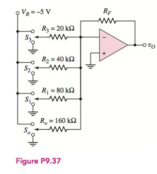
A summing amplifier can be used as a digital-to-analog converter (DAC).An example of a 4-bit DAC is shown in Figure P9.37. When switch S 3 isconnected to the − 5 V supply, the most significant bit is a 3 = 1 ; when S 3 isconnected to ground, the most significant bit is a 3 = 0 . The same conditionapplies to the other switches S 2 , S 1 , and S o , corresponding to bits a 2 , a 1 , and a o , where a o , is the least significant bit. (a) Show that the output voltage isgiven by v o = R F 10 [ a 3 2 + a 2 4 + a 1 8 + a 0 16 ] ( 5 ) where R F is in k Ω . (b) Find the value of R F such that v o = 2.5 V when thedigital input is a 3 a 2 a 1 a 0 = 1000 . (c) Using the results of part (b), find v o for: (i) a 3 a 2 a 1 a 0 = 0001 ,and(ii) a 3 a 2 a 1 a 0 = 1111 .
A summing amplifier can be used as a digital-to-analog converter (DAC).An example of a 4-bit DAC is shown in Figure P9.37. When switch S 3 isconnected to the − 5 V supply, the most significant bit is a 3 = 1 ; when S 3 isconnected to ground, the most significant bit is a 3 = 0 . The same conditionapplies to the other switches S 2 , S 1 , and S o , corresponding to bits a 2 , a 1 , and a o , where a o , is the least significant bit. (a) Show that the output voltage isgiven by v o = R F 10 [ a 3 2 + a 2 4 + a 1 8 + a 0 16 ] ( 5 ) where R F is in k Ω . (b) Find the value of R F such that v o = 2.5 V when thedigital input is a 3 a 2 a 1 a 0 = 1000 . (c) Using the results of part (b), find v o for: (i) a 3 a 2 a 1 a 0 = 0001 ,and(ii) a 3 a 2 a 1 a 0 = 1111 .
Solution Summary: The author explains the expression for the output voltage in Figure 1. Mark the values and redraw the circuit.
A summing amplifier can be used as a digital-to-analog converter (DAC).An example of a 4-bit DAC is shown in Figure P9.37. When switch
S
3
isconnected to the
−
5
V
supply, the most significant bit is
a
3
=
1
; when
S
3
isconnected to ground, the most significant bit is
a
3
=
0
. The same conditionapplies to the other switches
S
2
,
S
1
, and
S
o
, corresponding to bits
a
2
,
a
1
, and
a
o
, where
a
o
, is the least significant bit. (a) Show that the output voltage isgiven by
v
o
=
R
F
10
[
a
3
2
+
a
2
4
+
a
1
8
+
a
0
16
]
(
5
)
where
R
F
is in
k
Ω
. (b) Find the value of
R
F
such that
v
o
=
2.5
V
when thedigital input is
a
3
a
2
a
1
a
0
=
1000
. (c) Using the results of part (b), find
v
o
for: (i)
a
3
a
2
a
1
a
0
=
0001
,and(ii)
a
3
a
2
a
1
a
0
=
1111
.
QUESTION 2: Consider an ideal inverting op-amp in Figure P9.14.
Given R1 = 5 kN, R2 = 10.7 kN, and R1 = 3.6 kN. Input voltage is v7=
-0.76 V.
Determine vo, i2, i̟, and io.
vo (V)
i2 (HA)
Format : 5.3437
Format : -776
i (μA)
Format : 696.97339287623
io (HA)
Format : 904.94972275523
R2
R1
www
io
O vo
RL
Figure P9.14
a.
b.
C.
There is a dc-dc converter that provides isolation between input and
output current. Identify the converter type and describe the operation.
Draw the equivalent circuit to support the explanation. Assume the
converter operates in continuous-current mode.
Explain why a switched -mode dc-dc converter is better that a linear
regulator.
As an electrical engineer, you are required to design a chopper circuit
with an output voltage of 10 V from a 30 V input with switching
frequency of 50 kHz. The circuit is operated in continuous current, and
output ripple voltage is less than 0.8% with resistance load of 30 Q.
Assume the inductor value is 50 % larger than Lmin and assume ideal
components for this design. Identify the chopper type and construct
the circuit with IGBT as the power switching.
100 W at 60 V from a
Specify the
2 percent.
size.
Design a buck-boost converter to supply a load of
30 V source. The output ripple must be no more than
duty ratio, switching frequency,
inductor size, and capacitor
Need a deep-dive on the concept behind this application? Look no further. Learn more about this topic, electrical-engineering and related others by exploring similar questions and additional content below.


 Introductory Circuit Analysis (13th Edition)Electrical EngineeringISBN:9780133923605Author:Robert L. BoylestadPublisher:PEARSON
 Delmar's Standard Textbook Of ElectricityElectrical EngineeringISBN:9781337900348Author:Stephen L. HermanPublisher:Cengage Learning
 Programmable Logic ControllersElectrical EngineeringISBN:9780073373843Author:Frank D. PetruzellaPublisher:McGraw-Hill Education
 Fundamentals of Electric CircuitsElectrical EngineeringISBN:9780078028229Author:Charles K Alexander, Matthew SadikuPublisher:McGraw-Hill Education
 Electric Circuits. (11th Edition)Electrical EngineeringISBN:9780134746968Author:James W. Nilsson, Susan RiedelPublisher:PEARSON
 Engineering ElectromagneticsElectrical EngineeringISBN:9780078028151Author:Hayt, William H. (william Hart), Jr, BUCK, John A.Publisher:Mcgraw-hill Education,