
Videos
For the differential amplifier circuit ¡n Figure P17.1, neglect the base currents. (a) Determine
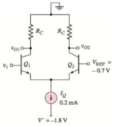
Figure P17.1
Want to see the full answer?
Check out a sample textbook solution
Chapter 17 Solutions
Microelectronics: Circuit Analysis and Design


- Determine the following. a. Forward path gainsb. Loop gainsc. Non touching loopsd. Transfer function output/ input.arrow_forward9. For the circuit shown in Figure Bl19a, Ve- 20V Rc 3k R = 10k 2 Wr VCE VBB=3V Figure B19a i) Sketch the DC load line in the Graph B19. ii) Calculate the Q point, if the zero signal base current is 50 µA and a -0.991. Mark the Q point in load line. D Focus 重 f8 fg f10 insort sc f12 & 近arrow_forwardConsider two LTI systems (cascade) with the unit sample responses p1(x) and P2[x].Compute output g(x) ... please check and guide as Figurearrow_forward
- Using 741 op amp, design a suitable circuit to generate Binary Phase Shift Keyiing(BFSK) modulator. Design should perform in such a way that the BFSK output should contain a frequency of f1=2kHz when message signal is low and f2 =4kHz when the message signal is high. Take the frequency of message signal as 200Hz. Draw the clear circuit diagram and calculate the values of resistors and capacitors used.arrow_forward1. Suppose that you have a 12-bit, successive approximation register (SAR) A/D converter with a total conversion time of 100 microseconds (including sampling time). a). What is the maximum frequency of an analog signal that it can capture? b). Suppose that the converter can convert an input voltage over the range of 0 to +3.3V, what is the minimum voltage change that should be measurable by this converter? c). What is the quantization error of the ADC?arrow_forwardQ1:-Design and connect astable 555 IC circuit and explain the output plot and VC.arrow_forward
- sampling Choose... Done Choose... measuring analog signal at equal interva.. ADC assign unique code DAC へarrow_forwardDefine in your own words what is a small signal FET when it comes to Av, Ai, ri, ro of the circuit.arrow_forwardapplication of bias circuits of the BJT in AC a. determine Zi and Zo b. Calculate Av and Ai c. repeat literal (a) with ro = 20k ohm d. repeat literal (b) with ro = 20k ohmarrow_forward
- 19. For the circuit shown in Figure B19a, Va 20V Rc= 3k2 RB = 10k2 VCE Figure B19a Sketch the DC load line in the Graph B19. Calculate the Q point, if the zero signal base current is 50 µA and a =0.991. Mark the Q point in load line. Graph B19 arch (hp 立arrow_forward2- For Zeigler-Nichols method the gain.. .. is increased till system oscillates at constant amplitude a) ki b) kp c) kaarrow_forwardDerive the output resistance using small signal model for the following circuits, assuming the transistor has output resistance of a transistor is ro and transconductance of gm. Rout PPA Rout Vb- Vbo Rout Rout Vdd Vb- Routarrow_forward
 Introductory Circuit Analysis (13th Edition)Electrical EngineeringISBN:9780133923605Author:Robert L. BoylestadPublisher:PEARSON
 Delmar's Standard Textbook Of ElectricityElectrical EngineeringISBN:9781337900348Author:Stephen L. HermanPublisher:Cengage Learning
 Programmable Logic ControllersElectrical EngineeringISBN:9780073373843Author:Frank D. PetruzellaPublisher:McGraw-Hill Education
 Fundamentals of Electric CircuitsElectrical EngineeringISBN:9780078028229Author:Charles K Alexander, Matthew SadikuPublisher:McGraw-Hill Education
 Electric Circuits. (11th Edition)Electrical EngineeringISBN:9780134746968Author:James W. Nilsson, Susan RiedelPublisher:PEARSON
 Engineering ElectromagneticsElectrical EngineeringISBN:9780078028151Author:Hayt, William H. (william Hart), Jr, BUCK, John A.Publisher:Mcgraw-hill Education,