
To design: The ECL circuit.
To find: All resistor values and the value of
Answer to Problem 17.2TYU
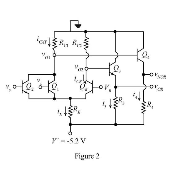
The redesign of the ECL circuit is shown in Figure 2 and the value of resistors are
Explanation of Solution
Calculation:
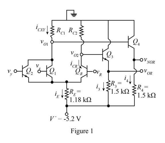
The given diagram is shown in Figure 1
The redesign circuit is shown below.
The required diagram is shown in Figure 2
The expression for
Substitute
If
The expression for
Substitute
Substitute
If
The expression for
Substitute
The expression for
Substitute
Input voltages
Substitute
If
Substitute
The expression for
Substitute
The value of
The expression for
Substitute
The expression for
Substitute
The expression for
Substitute
Conclusion:
Therefore, the redesign of the ECL circuit is shown in Figure 2 and the value of resistors are
Want to see more full solutions like this?
Chapter 17 Solutions
Microelectronics: Circuit Analysis and Design

- solve by impedancearrow_forwardConsider the circuit diagram below. Compute a single equivalent impedance for this circuit for a source frequency of F = 60 Hz. Express your final answer as a complex impedance with rectangular coordinates. You must show your all your work for the complex math. Include a diagram of the equivalent circuit as part of your solution.arrow_forwardConsider the circuit diagram below. Compute a single equivalent impedance for this circuit for a source frequency of f = 165 Hz. Express your final answer as a phasor with polar coordinates. You must show your all your work for the complex math. Include a diagram of the equivalent circuit as part of your solution.arrow_forward
- Consider the circuit diagram below. Using mesh analysis, compute the currents (a) IR1, (b) IL1, and (c) IC1. Express your final answers as phasors using polar coordinates with phase angles measured in degrees. Your solution should include the circuit diagram redrawn to indicate these currents and their directions. You must solve the system of equations using MATLAB and include the code or commands you ran as part of your solution.arrow_forwarduse kvl to solvearrow_forwardR1 is 978 ohms R2 is 2150 ohms R3 is 4780 R1 is parallel to R2 and R2 is parallel to R3 and R1 and R3 are in seriesarrow_forward
- Q7 For the circuit shown in Fig. 2.20, the transistors are identical and have the following parameters: hfe = 50, hie = 1.1K, hre = 0, and hoe = 0. Calculate Auf, Rif and Rof. Ans: 45.4; 112 KQ; 129. 25 V 10k 47k 4.7k Vo 150k w Vs 47k 4.7k W 22 5μF 33k 50uF 50μF 4.7k 4.7k R₁ Rof Rif R1000 Fig. 2.20 Circuit for Q7.arrow_forwardQ6)) The transistors in the feedback amplifier shown are identical, and their h-parameters are.. hie = 1.1k, hfe = 50, hre=o, and hoe = 0. Calculate Auf, Rif and Rof. {Ans: 6031583; 4. Kor. Is 4 4.7 k www 4.7k 91k 4.7k 91k 10k 1k. 10k 21000 4.7k w 15k Fig. 2.19 Circuit for Q6.arrow_forwardQ5 For the circuit shown in Fig. 2.18, hie =1.1 KQ, hfe =50. Find Avf, Rif and Rof Ans: -3.2; 193 ; 728 N. Vcc Vs Rs=10kQ Re=4KQ RF - = 40ΚΩ www Fig. 2.18 Circuit for Qs.arrow_forward
 Introductory Circuit Analysis (13th Edition)Electrical EngineeringISBN:9780133923605Author:Robert L. BoylestadPublisher:PEARSON
 Delmar's Standard Textbook Of ElectricityElectrical EngineeringISBN:9781337900348Author:Stephen L. HermanPublisher:Cengage Learning
 Programmable Logic ControllersElectrical EngineeringISBN:9780073373843Author:Frank D. PetruzellaPublisher:McGraw-Hill Education
 Fundamentals of Electric CircuitsElectrical EngineeringISBN:9780078028229Author:Charles K Alexander, Matthew SadikuPublisher:McGraw-Hill Education
 Electric Circuits. (11th Edition)Electrical EngineeringISBN:9780134746968Author:James W. Nilsson, Susan RiedelPublisher:PEARSON
 Engineering ElectromagneticsElectrical EngineeringISBN:9780078028151Author:Hayt, William H. (william Hart), Jr, BUCK, John A.Publisher:Mcgraw-hill Education,