
Videos
Consider the DTL circuit shown in Figure P17.19. Assume
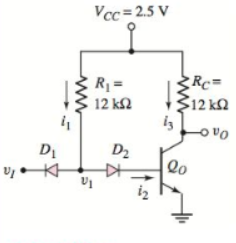
Figure P17.19
Want to see the full answer?
Check out a sample textbook solution
Chapter 17 Solutions
Microelectronics: Circuit Analysis and Design


- a) Find the list of mini terms f(W,X,Y,Z)b) Write the minimum function in maxi terms f(W,X,Y,Z)arrow_forwardAssignment-01 Write down the answers in an A4 paper. Make a PDF and rename with your student ID. Q1. Design a logic circuit using CMOS to implement the following function F(A, B, C) — А+(В+С B +C) Q2. Design a square wave generator using an operational amplifier that has oscillation frequency f=10 kHz and duty ratio D=40%.arrow_forwardThe following two figures shows an input signal and output signal for a given circuit. Which of the following circuits in the options can achieve this. Input signal V+42.42 V ον АА M 16.67 m Output signal V+41.72 V ον 16.67 m O Transformer O Half wave rectifier O Inverter None of the above V-0.318 V-13.27 V Time, |arrow_forward
- integrated circuit families (RTL, DTL, TTL, CMOS) 4. Let vx = vy = 0.1V (Logic 0), B = 25 Determine all the currents and voltages in the circuit below: 11, 12, iR, IRC, iB, v1 & vo. Vcc=5 V 84 48 = 4 ΚΩ VI Dx vx H Vy O KH Dy RB = 10 ΚΩ Figure 17.20 Basic diode-transistor logic gate D₁ D2₂ DA IRC VB ≤RC= 14 ΚΩ -OVO loarrow_forwardA) For the -K FFs shown below. Given the waveforms, Determine the Q output wave (PGT) CK B) Perform each of the following conversions: (0110.0000) BCD =(---s. (11100.1)2= (---- c d1001010) -6 (100010)- (-----)aray cod, (D3.E) 16- (-----) 2 BCD.arrow_forwardF(A, B, C, D) = m(0,3,5,8,10,12,13) + Ed (6,7,9,15) a) Implement the above function using a 2-1 multiplexer. Connect signal A to the multiplexer select input. Write expressions for the multiplexer inputs I0 and I1. b) Implement the above function using a 16-1 multiplexer. Write expressions inputs I0 to I15.arrow_forward
- integrated circuit families (RTL, DTL, TTL, CMOS) 4. Let vx = vy = 0.1V (Logic 0), B= 25 Determine all the currents and voltages in the circuit below: 11, 12, IR, IRC, iB, v1 & vo. Vcc=5 V 4₁R₁ = 4kQ2 D₁ D₂ VI VB IRC ww Rc= 4 ΚΩ Dx Vx o Vy H RB = Dy 10 km2 Figure 17.20 Basic diode-transistor logic gate Ovo learrow_forwardENT-139 Digital Circuits Spring 2021/2022 7. Determine the expression of the output x, then simplify the expression. A 8. Simplify the expression X = ĀBC + ABC + BCD, then draw the simplified circuit. 9. Simplify the expression X = (Ā + B)(A + B), then draw the simplified circuit. 10.Simplify the expression X = (M + N)(M + P)(N + P), then draw the simplified circuit.arrow_forwardintegrated circuit families (RTL, DTL, TTL, CMOS) 4. Let vx = vy = 0.1V (Logic 0), B = 25 Determine all the currents and voltages in the circuit below: 11, 12, IR, IRC, iB, v1 & vo. Vcc=5 V VX Vy O- Dx KH KH Dy R = 4 ΚΩ D₁ VI 12 VB www iRC. Rg= 10 ΚΩ ≤Rc= 4 ΚΩ -OVOarrow_forward
- Question: 18 The time difference between the input signal crossing a 0.5VDD and the output signal crossing its 0.5 VDD when the output signal is changing from low to high is --- A. Propagation Delay low-to-high (Rise Propagation) B. Fall Transition Time C. Rise Transition Time D. Propagation delay high-to-low (Fall Propagation)arrow_forwardA major advantage of PRTS is that they are very linear. A disadvantage is that they have poor sensitivity. Select one: True Falsearrow_forwardwrite an introduction and objective for SSB modulationarrow_forward
 Introductory Circuit Analysis (13th Edition)Electrical EngineeringISBN:9780133923605Author:Robert L. BoylestadPublisher:PEARSON
 Delmar's Standard Textbook Of ElectricityElectrical EngineeringISBN:9781337900348Author:Stephen L. HermanPublisher:Cengage Learning
 Programmable Logic ControllersElectrical EngineeringISBN:9780073373843Author:Frank D. PetruzellaPublisher:McGraw-Hill Education
 Fundamentals of Electric CircuitsElectrical EngineeringISBN:9780078028229Author:Charles K Alexander, Matthew SadikuPublisher:McGraw-Hill Education
 Electric Circuits. (11th Edition)Electrical EngineeringISBN:9780134746968Author:James W. Nilsson, Susan RiedelPublisher:PEARSON
 Engineering ElectromagneticsElectrical EngineeringISBN:9780078028151Author:Hayt, William H. (william Hart), Jr, BUCK, John A.Publisher:Mcgraw-hill Education,