Electronics Fundamentals: Circuits, Devices & Applications
8th Edition
ISBN: 9780135072950
Author: Thomas L. Floyd, David Buchla
Publisher: Prentice Hall
expand_more
expand_more
format_list_bulleted
Videos
Textbook Question
Chapter 17, Problem 37P
Each E-MOSFET in Figure 17-83 has a
Expert Solution & Answer
Want to see the full answer?
Check out a sample textbook solution
Students have asked these similar questions
List the differences between D-MOSFETs and E-MOSFETs.
* In a pnp transistor, the
p regions are
base and emitter O
base and collector
emitter and collector
* An SCR can be turned off by
forced commutation O
a negative pulse on the gate
anode current interruption
forced commutation and anode current interruption O
The region in the output characteristics of JFET where the Drain current (Ip) is directly
proportional to the Drain Source voltage (VDs) is called
10
A D-MOSFET is considered to be a normally
device
Chapter 17 Solutions
Electronics Fundamentals: Circuits, Devices & Applications
Ch. 17 - In a bipolar transistor, if the base-emitter...Ch. 17 - When a transistor is saturated. an increase in...Ch. 17 - Prob. 3TFQCh. 17 - The power gain of a CC amplifier is the same as...Ch. 17 - A class B amplifier is more efficient than a class...Ch. 17 - A JFET is always operated with the gate-source...Ch. 17 - Prob. 7TFQCh. 17 - The transconductance of a FET is the ratio of ac...Ch. 17 - Prob. 9TFQCh. 17 - The input to a feedback oscillator is only the...
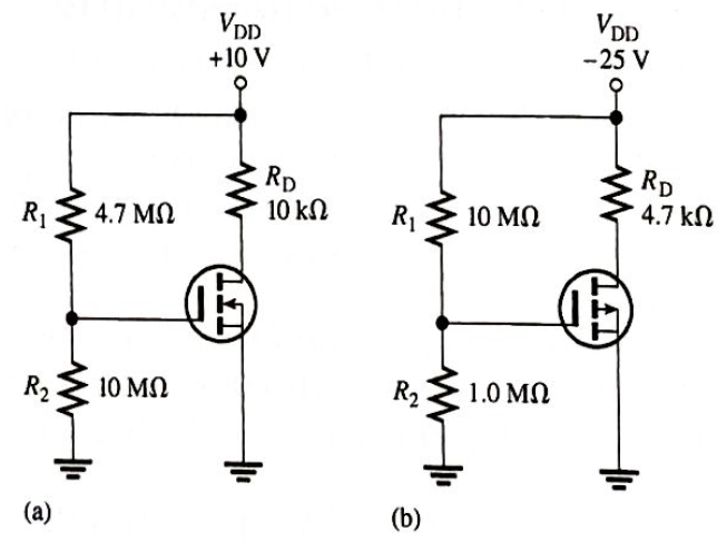
Ch. 17 - The n-type regions in an npn bipolar junction...Ch. 17 - The n-region in a pnp transistor is the base...Ch. 17 - Prob. 3STCh. 17 - Prob. 4STCh. 17 - Prob. 5STCh. 17 - Alpha () is the ratio of collector current to...Ch. 17 - If the beta of a certain transistor operating in...Ch. 17 - If the base current of a transistor operating in...Ch. 17 - Prob. 9STCh. 17 - When the gate-to-source voltage of an n-channel...Ch. 17 - When a negative gate-to-source voltage is applied...Ch. 17 - Prob. 12STCh. 17 - If the capacitor from emitter to ground in a CE...Ch. 17 - When the collector resistor in a CE amplifier is...Ch. 17 - The input resistance of a CE amplifier is affected...Ch. 17 - The output signal of a CE amplifier is always in...Ch. 17 - The output signal of a common-collector amplifier...Ch. 17 - The largest theoretical voltage gain obtainable...Ch. 17 - In a class A amplifier, the output signal is...Ch. 17 - A class A amplifier conducts for 90 of input cycle...Ch. 17 - Prob. 21STCh. 17 - Feedback oscillators operate on the principle of...Ch. 17 - What is the value of IC for IE=5.34mA and IB=475A?Ch. 17 - Prob. 2PCh. 17 - Prob. 3PCh. 17 - In a certain transistor circuit, the base current...Ch. 17 - Find IB,IE, and in Figure 17-70 given that DC=0.98...Ch. 17 - The transistor in Figure 17-70 is replaced with...Ch. 17 - Prob. 7PCh. 17 - Prob. 8PCh. 17 - Determine IB,IC, and VC in Figure 17-72.Ch. 17 - For the circuit in Figure 17-73, find VB,VE,IE,IC,...Ch. 17 - In Figure 17-73, what is VCE? What are the Q-point...Ch. 17 - A transistor amplifier has a voltage gain of 50....Ch. 17 - To achieve an output of 10 V with an input of300...Ch. 17 - A 50 mV signal is applied to the base of a...Ch. 17 - Determine the voltage gain for Figure 17-74.Ch. 17 - Determine each of the dc voltages, VB,VC, and VE,...Ch. 17 - Determine the following dc values for the...Ch. 17 - Determine the following ac values for the...Ch. 17 - The amplifier in Figure 17-76 has a variable gain...Ch. 17 - If a load resistance of 600 is placed on the...Ch. 17 - Determine the voltage gain for the...Ch. 17 - What is the total input resistance in Figure...Ch. 17 - A load resistance is capacitively coupled in the...Ch. 17 - Prob. 24PCh. 17 - Determine the maximum peak output voltage and peak...Ch. 17 - The efficiency of a certain class B push-pull...Ch. 17 - Prob. 27PCh. 17 - The transistor in Figure 17-80 has a DC of 150....Ch. 17 - The VGS of ap-channel JFET is increased from 1 V...Ch. 17 - Why must the gate-to-source voltage of an...Ch. 17 - Draw the schematic symbols for n-channel and...Ch. 17 - Explain why both types of MOSFETs have an...Ch. 17 - In what mode is an n-channel D-MOSFET operating...Ch. 17 - A certain E-MOSFET has a VGS(th)=3V. What is the...Ch. 17 - For each circuit in Figure 17-81, determine VDS...Ch. 17 - Prob. 36PCh. 17 - Each E-MOSFET in Figure 17-83 has a VGS(th) of +5...Ch. 17 - Prob. 38PCh. 17 - Find the gain of each amplifier in Figure 17-85.Ch. 17 - Determine the gain of each amplifier in Figure...Ch. 17 - If the voltage gain of the amplifier portion of a...Ch. 17 - Generally describe the change required to the...Ch. 17 - Prob. 43PCh. 17 - Prob. 44PCh. 17 - Prob. 47PCh. 17 - Prob. 48PCh. 17 - Prob. 49PCh. 17 - Prob. 50PCh. 17 - Prob. 51PCh. 17 - Prob. 52PCh. 17 - Open file P17-53. Determine if the circuit is...
Knowledge Booster


Learn more about
Need a deep-dive on the concept behind this application? Look no further. Learn more about this topic, electrical-engineering and related others by exploring similar questions and additional content below.Similar questions
- In n-channel JFET, at pinch off voltage, the drain current isarrow_forwardThe p regions in a pnp transistor are emitter and collector collector and base emitter and basearrow_forwardFind the operating region of the MOSFET and Vn when In = 0.2A and R=5 ohm? +1.8 V R o Vp O a. None- off the options O b. Cut-off, Vp = 0.8V O c. Triode, Vp = 0.6V O d. Saturation, Vp = 0.8Varrow_forward
- COMMON EMITTER What will be the effect on the output voltage if we change the value of the following components? a. collector resistor, Rc b. bypass capacitor c. no bypass capacitorarrow_forwardThe two transistor model of the SCR can obtained by O a. bisecting the SCRS top two & bottom two layers O b. bisecting the SCR vertically O c. bisecting the SCRS middle two layers O d. bisecting the SCR horizontallyarrow_forwardspecified Pinch- off Voltage of =0, what is Vos at the 91 A JFET has a 5 V. when Vos Point where the drain current become Constant?arrow_forward
- Small amount of space it takes on a chip O All of the above 7. The main types of field effect transistor are O BJT and FET O UJT and FET O JFET and MOSFET O None of the above 9.The arrow on the symbol of MOSFET indicat that it is a N-channel MOSFET the direction of electrons O the direction of conventional current flow O that it is a P-channel MOSFETarrow_forwardA fixed bias n-channel JFET with Vdd= 12V, Rd= 1.2k ohms. Idss=12mA and Vp=-4V. Determine Vs. a.0 V b.None of these c.4.35V d.6.7Varrow_forwardRedraw the JFET in the figure below showing how to connect a bias voltage between the gate and source. +VDD Rparrow_forward
- Create a circuit design for 2.4V output voltage divider, Create a circuit design for 8V output voltage divider, Create a circuit design for 0.571A output current divider and Create a circuit design for 0.176A output current divider.arrow_forwardWhat is the Q-point for a biased transistor as in Figure F with Ig = 70μA, BDC 110, Vcc = 24V, and Rc = 3k2. 3kohm Rc= 01 Vout 2N2222A RB w IB = 70μΑ BDC= 110 VBB Figure F Vcc = 24Varrow_forwardShown below is a section from the datasheet of 74LS32, a quad 2-input OR chip. What is the noise margin high (in V) of this chip? Limits Symbol Parameter Min Typ Max Unit VIH Input HIGH Voltage 2.0 V VIL Input LOW Voltage V 0.8 VIK Input Clamp Diode Voltage -0.65 -1.5 V V VOH Output HIGH Voltage 3.5 V V VOL Output LOW Voltage 0.35 0.5 V 20 μA IH Input HIGH Current 0.1 mA IIL Input LOW Current -0.4 mA los Short Circuit Current (Note 1) -100 mA Power Supply Current Icc 6.2 Total, Output HIGH mA Total, Output LOW 9.8 74 74 74 2.7 -20arrow_forward
arrow_back_ios
SEE MORE QUESTIONS
arrow_forward_ios
Recommended textbooks for you
 Introductory Circuit Analysis (13th Edition)Electrical EngineeringISBN:9780133923605Author:Robert L. BoylestadPublisher:PEARSON
 Delmar's Standard Textbook Of ElectricityElectrical EngineeringISBN:9781337900348Author:Stephen L. HermanPublisher:Cengage Learning
 Programmable Logic ControllersElectrical EngineeringISBN:9780073373843Author:Frank D. PetruzellaPublisher:McGraw-Hill Education
 Fundamentals of Electric CircuitsElectrical EngineeringISBN:9780078028229Author:Charles K Alexander, Matthew SadikuPublisher:McGraw-Hill Education
 Electric Circuits. (11th Edition)Electrical EngineeringISBN:9780134746968Author:James W. Nilsson, Susan RiedelPublisher:PEARSON
 Engineering ElectromagneticsElectrical EngineeringISBN:9780078028151Author:Hayt, William H. (william Hart), Jr, BUCK, John A.Publisher:Mcgraw-hill Education,
Introductory Circuit Analysis (13th Edition)
Electrical Engineering
ISBN:9780133923605
Author:Robert L. Boylestad
Publisher:PEARSON
Delmar's Standard Textbook Of Electricity
Electrical Engineering
ISBN:9781337900348
Author:Stephen L. Herman
Publisher:Cengage Learning
Programmable Logic Controllers
Electrical Engineering
ISBN:9780073373843
Author:Frank D. Petruzella
Publisher:McGraw-Hill Education
Fundamentals of Electric Circuits
Electrical Engineering
ISBN:9780078028229
Author:Charles K Alexander, Matthew Sadiku
Publisher:McGraw-Hill Education
Electric Circuits. (11th Edition)
Electrical Engineering
ISBN:9780134746968
Author:James W. Nilsson, Susan Riedel
Publisher:PEARSON
Engineering Electromagnetics
Electrical Engineering
ISBN:9780078028151
Author:Hayt, William H. (william Hart), Jr, BUCK, John A.
Publisher:Mcgraw-hill Education,
How a MOSFET Works - with animation! | Intermediate Electronics; Author: CircuitBread;https://www.youtube.com/watch?v=Bfvyj88Hs_o;License: Standard Youtube License