
Videos
The parameters of the TIL NAND circuit in Figure 17.24 are:
(a)
The value of the base and the collector current in each of the transistor.
Answer to Problem 17.9EP
The value of the currents are
Explanation of Solution
Calculation:
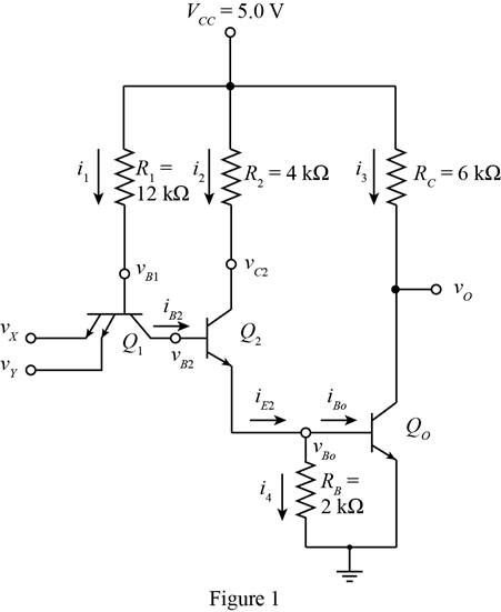
The given diagram is shown in Figure 1.
The expression for the voltage
Substitute
The second transistor and the transistor at the output are both cut off, then the base voltage
Substitute
The expression for the value of the current
Substitute
The expression to determine the value of the base current
Substitute
The transistor two and the output transistor are cutoff, therefore the value of the current are given by,
The expression for the value of the current
Conclusion:
Therefore, the value of the currents are
(b)
The value of the base and the collector current in each of the transistor.
Answer to Problem 17.9EP
The value of the currents are
Explanation of Solution
Calculation:
The input transistor is biased with inverse active mode when the input voltage is
The expression for the voltage
Substitute
The expression to determine the value of the collector voltage is given by,
Substitute
The expression to determine the value of the current
Substitute
The expression to determine the value of the base current
Substitute
The expression to determine the value of the current
Substitute
The expression to determine the value of the collector current
Substitute
The expression to determine the value of the current
Substitute
The expression to determine the value of the base current
Substitute
The expression to determine the value of the base current
Substitute
The expression to determine the value of the current
Substitute
The expression to determine the value of the current
Substitute
The expression to determine the value of the current
Substitute
Conclusion:
Therefore, the value of the currents are
Want to see more full solutions like this?
Chapter 17 Solutions
MICROELECT. CIRCUIT ANALYSIS&DESIGN (LL)


- 10) In an N-channel JFET, pinch-off occurs when the gate bias is zero. 11) When a transistor is conducting as much as it possibly can, it is said to be at cutoff. 12) A bipolar transistor has three P-N junctions. 13) In a PNP circuit, the collector is positive with respect to the emitter. 14) The output is in phase with the input in a common-emitter circuit. 15) Adding emitter resistance in a BJT amplifier increases the stability of the output.arrow_forwardWe can calculate the transconductance parameter gm of a MOS transistor, if we know either its Gate-Source voltage or its Drain current. True or False if we know the early voltage of a MOSFET, we can calculate the channel length modulation parameterarrow_forward7. Sketch the transfer characteristics of a n-channel depletion-type MOSFET if Vp= -5V and IDSS =10mAarrow_forward
- For a PCM signal, Compute L, if the compression parameter µ=100 and the minimum SNR required is 45dB.Determine the output SQNR with this value of L. Remember that L must be a power of 2,that is, L=2n for a binary PCM.arrow_forwardConsider an NPN BJT with the following parameters: Ien = 1 mA, IEp = 0.01 mA, Icn = 0.98 mA, Icp = 0.0001 mA %3D (1) Determine the currents, IE, lc, IB. (2) Determine the emitter injection efficiency, Y. (3) Determine the base transport factor, B'. (4) Determine ɑpc, Boc.arrow_forwardThe Miller capacitance in BJT transistors is related to Оа. O a. ľu. O b. rr. O c. Cu. O d. C.arrow_forward
- Explain the transistor amplifying action of a common-base npn transistor with proper biasing arrangement. Consider α=0.98 Don,t copy from anywhere.Must do step by step.Must draw diagramarrow_forwardThe common-emitter output characteristics for annpn transistor are given . What are thevalues of βF at (a) IC = 5 mA and VC E = 5 V?(b) IC = 7 mA and VC E = 7.5 V? (c) IC = 10 mAand VC E = 14 V?arrow_forwardState whether the following statement is true or false. “The curvature in the output voltage of a bandgap reference circuit occurs mainly due to the non-linearity in the PTAT current.”arrow_forward
- 5. Choose the correct answer: a) The reason of high input resistance of the MOSFET is: 1. The insulator layer. 2. The reverse biasing. 3. The forward biasing. b) Which transistor has no Ipss parameter?. 1. JFET. 2. E-MOSFET. 3. D-MOSFET. ¢) For an n-channel D-MOSFET transistor, at what condition can gm be greater than gmo?. 1. Vs is positive. 2. Vgs is negative. 3. Vas =0. d) A certain amplifier has an Rp=1KQ. When a load resistance of 1KQ is capacitively coupled to the drain, the gain will reduce to the: 1. Half. 2. Quarter. 3. Not change.arrow_forwardThe parameters of the transistor below are VTN= 0.6 V and K = 0.5 mA/V?, find the value of R1, R2, Rp such that Ipq = 0.5689 mA, VpsQ = 1 V and R1+R=90 k2. Sketch the load line and plot the Q-point. v+ = +2.5 V Rp R1 R2 V-=-2.5 V wwarrow_forwardThe parameters of the transistor below are VTN = 0.6 V and Ka = 0.5 mA/V?, find the value of R1, R2, Rp such that IpDQ = 0.5689 mA, VDSQ = 1 V and R1+R=90 k2. Sketch the load line and plot the Q-point. v*= +2.5 V Rp R R2 V---2.5 V wwarrow_forward
 Introductory Circuit Analysis (13th Edition)Electrical EngineeringISBN:9780133923605Author:Robert L. BoylestadPublisher:PEARSON
 Delmar's Standard Textbook Of ElectricityElectrical EngineeringISBN:9781337900348Author:Stephen L. HermanPublisher:Cengage Learning
 Programmable Logic ControllersElectrical EngineeringISBN:9780073373843Author:Frank D. PetruzellaPublisher:McGraw-Hill Education
 Fundamentals of Electric CircuitsElectrical EngineeringISBN:9780078028229Author:Charles K Alexander, Matthew SadikuPublisher:McGraw-Hill Education
 Electric Circuits. (11th Edition)Electrical EngineeringISBN:9780134746968Author:James W. Nilsson, Susan RiedelPublisher:PEARSON
 Engineering ElectromagneticsElectrical EngineeringISBN:9780078028151Author:Hayt, William H. (william Hart), Jr, BUCK, John A.Publisher:Mcgraw-hill Education,