
(a)
The value of the current and voltage
(a)
Answer to Problem 17.15P
The value of the current
Explanation of Solution
Calculation:
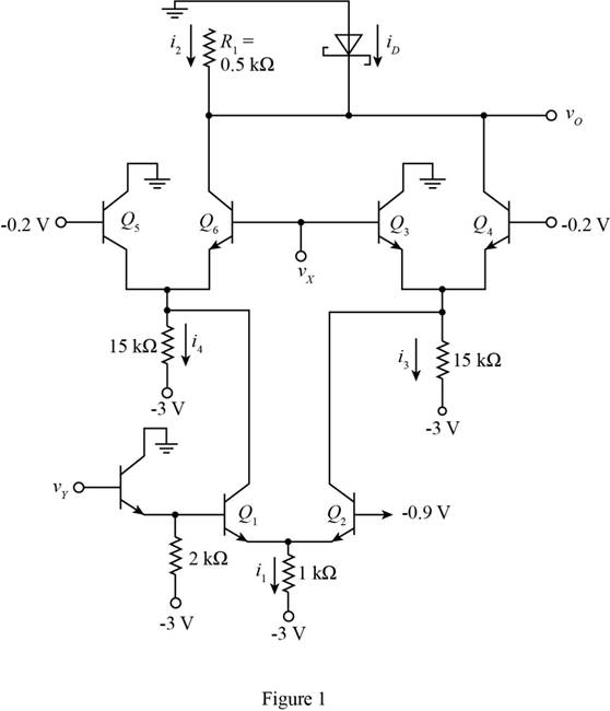
The given diagram is shown in Figure 1.
The expression for the current
Substitute
The expression to determine the value of the current
Substitute
The expression to determine the value of the current
Substitute
The expression for the value of the current
Substitute
The expression to determine the value of the current
Substitute
The output voltage is the voltage of the diode with opposite polarity and is given by,
Conclusion:
Therefore, the value of the current
(b)
The value of the current and voltage
(b)
Answer to Problem 17.15P
The value of the current
Explanation of Solution
Calculation:
The diode
The expression for the current
Substitute
The expression to determine the value of the current
Substitute
The expression to determine the value of the current
Substitute
The expression to determine the value of the current
Substitute
The expression to determine the value of the output voltage is given by,
Substitute
Conclusion:
Therefore, the value of the current
(c)
The value of the current and voltage
(c)
Answer to Problem 17.15P
The value of the current
Explanation of Solution
Calculation:
The transistor
The expression for the current
Substitute
The expression to determine the value of the current
Substitute
The expression to determine the value of the current
Substitute
The diode is in the cut off and the diode current is given by,
The expression to determine the value of the current
Substitute
The expression to determine the value of the output voltage is given by,
Substitute
Conclusion:
Therefore, the value of the current
(d)
The value of the current and voltage
(d)
Answer to Problem 17.15P
The value of the current
Explanation of Solution
Calculation:
The transistor
The expression for the current
Substitute
The expression to determine the value of the current
Substitute
The expression to determine the value of the current
Substitute
The expression for the value of the current
Substitute
The expression to determine the value of the current
Substitute
The output voltage is the voltage of the opposite polarity and is given by,
Conclusion:
Therefore, the value of the current
Want to see more full solutions like this?
Chapter 17 Solutions
MICROELECT. CIRCUIT ANALYSIS&DESIGN (LL)

- %3D For the circuit shown in Figure B23, a = 0.97, calculate the following: i. Collector current (Ic) ii. Collector-Base voltage (VCB) iii. Emitter Current (IE) iv. Base Current (IB) IE Ic 2.5 k2 Ouput 2.8V IB 10V VEE Vcc Figure B23arrow_forwardThe voltage waveforms shown below are obtained from a three-phase power rectifier used in an ESKOM application.The rectifier output before the inductive filter is denoted by VL and the load voltage after the inductive filter by Vo. Ignore any diode losses and consider a load resistance of 12.7 Ω. Analyse the waveforms and specify / calculate,11) the supply frequency;12) the rectifier pulse number;13) the rectifier average output voltage;14) the average output current;15) the r.m.s. value of the output current;16) the r.m.s. value of the harmonics present in the output current;17) the dc current rating of the rectifier diodes;18) the r.m.s. current rating of the rectifier diodes;19) the peak repetitive reverse voltage rating of the rectifier diodes;20) the peak repetitive forward current rating of the rectifier diodes;21) the line-line r.m.s. voltage of the three-phase supply;22) the rectification efficiency of the converter;23) the converter transformer utilisation factor;arrow_forwardQuestion 2 a) Briefly explain the de chopper, inverter, controlled rectifier and ac voltage controller. b) A buck-boost regulator as shown in Figure 2 has an input voltage, Vs = 12 V. The duty cycle, k = 0.35 and the switching frequency is 30 kHz. It also has an inductance, L = 200 µH, filter capacitance, C = 440 µF. The average load current, Ia 1.25 A. Determine the: i. average output voltage, Va, ii. peak-to-peak output ripple voltage, AVc, iii. peak-to-peak output ripple current of inductor, AI, iv. peak current of the transistor, Ip, V. critical values of L and C, and vi. critical values of L and C if Vs is increased to 14 V. Estimate the change in percentage for the critical values of L and C. is Vs C Load Vo, Vs VC i, Ia Figure 2arrow_forward
- Discuss the operation of an LM317 IC regulator.arrow_forwardFor the circuit shown in Figure B23, a- 0.97, calculate the following: i. Collector current (Ic) ii. Collector-Base voltage (Ven) i. Emitter Current (I) iv. Base Current (In) Ic 2.5 kl Ouput 2.8V IB 10V Vecarrow_forwardPLEASE explain this MCQ ASAParrow_forward
- ece Discuss the operation of an LM317 IC regulator.arrow_forwardA 4:1 transformer is connected to a bridge rectifier circuit with a lkn load. What is the peak output current of the circuit if the input voltage is 250Vrms? Express your answer in mA.arrow_forwardAt high levels of gate current, the characteristics of an SCR approach those of what semiconductor device? a. MOSFET b. BJT c. JFET d. Diodearrow_forward
- 1. Briefly describe what a Schottky junction is and how it is formed. Draw the energy band diagrams of a Schottky junction under equilibrium, forward bias, and reverse bias.arrow_forward1. Derive a Boole an expression for the following digital circuitarrow_forwardVDD = 16V, VGG = -3V, RG = 1.2 M-ohm, RD = 2200ohm, IDSS = 10mA, VP=-4.5V a. Determine the drain current ID in mA. b. Determine the gate voltage, VG c. Determine the source terminal voltage, VS d. Determine the gate-to-source voltage, VGS e. Calculate the drain terminal voltage, VD f. Determine the drain-to-source voltage, VDSarrow_forward
 Introductory Circuit Analysis (13th Edition)Electrical EngineeringISBN:9780133923605Author:Robert L. BoylestadPublisher:PEARSON
 Delmar's Standard Textbook Of ElectricityElectrical EngineeringISBN:9781337900348Author:Stephen L. HermanPublisher:Cengage Learning
 Programmable Logic ControllersElectrical EngineeringISBN:9780073373843Author:Frank D. PetruzellaPublisher:McGraw-Hill Education
 Fundamentals of Electric CircuitsElectrical EngineeringISBN:9780078028229Author:Charles K Alexander, Matthew SadikuPublisher:McGraw-Hill Education
 Electric Circuits. (11th Edition)Electrical EngineeringISBN:9780134746968Author:James W. Nilsson, Susan RiedelPublisher:PEARSON
 Engineering ElectromagneticsElectrical EngineeringISBN:9780078028151Author:Hayt, William H. (william Hart), Jr, BUCK, John A.Publisher:Mcgraw-hill Education,