
Concept explainers
(a)
The base and the collector current in each of the transistor. Also, the power dissipation in the gate.
(a)
Answer to Problem 17.12EP
The currents in the transistors are,
Explanation of Solution
Calculation:
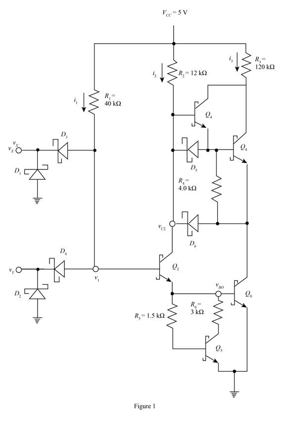
The given diagram is shown in Figure 1
The expression to determine the value of the voltage
Substitute
The expression to determine the value of the current
Substitute
The conversion from
The conversion from
The second transistor and the output transistor are in cut off region and the current in the circuit are given by,
The expression for the value of the collector current and the base current of the output transistor is given by,
The expression for the base and the collector current of the third and the fourth transistor are given by,
The expression for the power dissipated in the circuit is given by,
Substitute
Conclusion:
Therefore, the currents in the transistors are,
(b)
The base and the collector current in each of the transistor. Also, the power dissipation in the gate.
(b)
Answer to Problem 17.12EP
The currents in the transistors are,
Explanation of Solution
Calculation:
The expression to determine the value of the voltage
Substitute
The expression for the voltage
Substitute
The expression to determine the value of the current
Substitute
The expression to determine the value of the current
Substitute
The conversion from
The conversion from
The expression for the base current of the second transistor is given by,
Substitute
The expression for the collector current of the second transistor is given by,
Substitute
The fifth transistor is in the cut off region and the current in the circuit are given by,
The expression for the value of the collector current of output transistor is given by,
Substitute
The expression for the base and the collector current of the third and the fourth transistor are given by,
The expression for the power dissipated in the circuit is given by,
Substitute
The conversion from
The conversion from
Conclusion:
Therefore, the currents in the transistors are,
Want to see more full solutions like this?
Chapter 17 Solutions
MICROELECT. CIRCUIT ANALYSIS&DESIGN (LL)


- 1. A SCR has a forward breakover voltage of 175V when a gate pulse of 2 mA is made to flow. Find the conduction angle if a sinusoidal voltage of 350 V peak is applied.arrow_forwardFor the circuit shown in Figure B23, a- 0.97, calculate the following: i. Collector current (Ic) ii. Collector-Base voltage (Ven) i. Emitter Current (I) iv. Base Current (In) Ic 2.5 kl Ouput 2.8V IB 10V Vecarrow_forwardintegrated circuit families (RTL, DTL, TTL, CMOS) 4. Let vx = vy = 0.1V (Logic 0), B = 25 Determine all the currents and voltages in the circuit below: 11, 12, iR, IRC, iB, v1 & vo. Vcc=5 V 84 48 = 4 ΚΩ VI Dx vx H Vy O KH Dy RB = 10 ΚΩ Figure 17.20 Basic diode-transistor logic gate D₁ D2₂ DA IRC VB ≤RC= 14 ΚΩ -OVO loarrow_forward
- The analog input channel voltage range for a PIC16 Microcontroller is limited to the positive range 0-Vref. Many situations require a digitized mapping from bipolar analog signals to unipolar signals. A simple resistive network has been designed to translate a bipolar voltage range of ±10V to a unipolar range of 0-6.6 V, assuming Vref is +6.6 V. A reasonable resistor combination is: a. None of them b. 2.212, 2.70, and 5 Kohms c. 2.212, 2.70, and 2.70 Kohms d. 1.122, 1.70, and 3.30 Kohmsarrow_forwardThe gate characteristic of an SCR has a straight-line slope of 125. What should be the gate-source resistance, if the source triggering voltage is 12 V and allowable value of gate power dissipation is 0.65 watts. (a) 450 2 (b) 291.36 2 (c) 41.46 2 (d) 83.54 2arrow_forwardSketch each of the following special digital sequences: a. 58 (n) b. -28 (n-5) c. -5u(n) d. 5u(n-2)arrow_forward
- For the circuit shown in Figure B23, a = 0.97, %3D calculate the following: i. Collector current (Ic) ii. Collector-Base voltage (VCB) iii. Emitter Current (IE) iv. Base Current (IB) IE Ic 2.5 k Ouiput 2.8V IB 10V VEE Vcc Figure B23arrow_forwardn the SCR structure the gate terminal is located a. near the cathode terminal b. near the anode terminal c. in between the anode & cathode terminal d. in between the collector & emitter terminalarrow_forward5. The Base current is 15µA and B=147 for an NPN transistor. Calculate emitter current.arrow_forward
 Introductory Circuit Analysis (13th Edition)Electrical EngineeringISBN:9780133923605Author:Robert L. BoylestadPublisher:PEARSON
 Delmar's Standard Textbook Of ElectricityElectrical EngineeringISBN:9781337900348Author:Stephen L. HermanPublisher:Cengage Learning
 Programmable Logic ControllersElectrical EngineeringISBN:9780073373843Author:Frank D. PetruzellaPublisher:McGraw-Hill Education
 Fundamentals of Electric CircuitsElectrical EngineeringISBN:9780078028229Author:Charles K Alexander, Matthew SadikuPublisher:McGraw-Hill Education
 Electric Circuits. (11th Edition)Electrical EngineeringISBN:9780134746968Author:James W. Nilsson, Susan RiedelPublisher:PEARSON
 Engineering ElectromagneticsElectrical EngineeringISBN:9780078028151Author:Hayt, William H. (william Hart), Jr, BUCK, John A.Publisher:Mcgraw-hill Education,