
Concept explainers
Videos
The saturated output voltages are ±VP for the Schmitt trigger in Figure P15.47. (a) Derive the expressions for the crossover voltages VTH and VTL (b) if VP=12V , VREF=−10V , and R3=10kΩ , find R1 and R2 such that the switching point is VS=−5V and the hysteresis width is 0.2 V. (c) Sketch the voltage transfer characteristics.
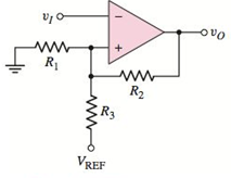
Figure P15.47
(a)
To find: The expression for given crossover voltages.
Answer to Problem 15.47P
The upper crossover voltage of Schmitt trigger is VTH=VREFR3+VPR21R1+1R2+1R3
The lower crossover voltage of Schmitt trigger is VTL=VREFR3−VPR21R1+1R2+1R3
Explanation of Solution
Given:
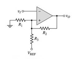
The given circuit is shown below.
Calculation:
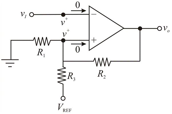
From the above circuit
The inverting node is, v+=vi
Applying Kirchhoff's current law at non-inverting node:
v+R1+v+−voR2+v+−VREFR3=0
v+R1+v+R2−voR2+v+R3−VREFR3=0
v+[1R1+1R2+1R3]−voR2−VREFR3=0
v+[1R1+1R2+1R3]=VREFR3+voR2
v*=VREFR3+voR21R1+1R2+1R3
Substitute v+=v, in the above equation,
vl=VRFFR3+voR21R1+1R2+1R3……
When vo=VP and vI=VTH in equation-(1),
The upper crossover voltage of Schmitt trigger is VTH=VREFR3+VPR21R1+1R2+1R3
When vo=−Vp and vt=VTL in equation-(1)
The lower crossover voltage of Schmitt trigger is VTL=VREFR3−VPR21R1+1R2+1R3
Conclusion:
The upper crossover voltage of Schmitt trigger is VTH=VREFR3+VPR21R1+1R2+1R3
The lower crossover voltage of Schmitt trigger is VTL=VREFR3−VPR21R1+1R2+1R3
(b)
To find: The values of R1 and R2
Answer to Problem 15.47P
The required values are R1=10.17kΩ and R2=600kΩ
Explanation of Solution
Given:
Saturated output voltage is, VP=12V
Reference voltage is, VREF=−10V
One resistor value is, R3=10kΩ
Switching point is, Vs=−5V
Hysteresis width is VTH−VTL=0.2V
Calculation:
Substitute Vp,VREF and R3 in upper crossover voltage,
VTH=−1010×103+12R21R1+1R2+110×103
Hence, VTH=−1010×103+12R21R1+1R2+110×103
Substitute Vp,VREF and R3 in lower crossover voltage,
VTL=−1010×103−12R21R1+1R2+110×103
Substitute VTH and VTL in equation VTH−VTL=−1010×103+12R21R1+1R2+110×103−−1010×103−12R21R1+1R2+110×103
−1010×103+12R21R1+1R2+110×103−−1010×103−12R21R1+1R2+110×103=0.2
11R1+1R2+110×103(−1010×103+12R2−(−1010×103−12R2))=0.2
11R1+1R2+110×103(−1010×103+12R2+1010×103+12R2)=0.2
11R1+1R2+110×103(24R2)=0.2
24R2=0.2(1R1+1R2+110×103)
240.2=R2(1R1+1R2+110×103)
120=R2(1R1+1R2+110×103).......(3)
Assuming VH and VL are symmetrical about zero. The switching voltage becomes,
Vs=VREFR31R1+1R2+1R3−5=110×1031R1+1R2+110×1035=101R1+1R2+110×1031R1+1R2+110×103=1010×10351R1+1R2+110×103=15×103
Hence, we get 1R1+1R2+110×103=15×103
Substitute 1R1+1R2+110×103=15×103 in equation- (3)
120=R2(15×103)R2=120(5×10³)R2=600×103
Therefore, value of R2 is R2=600kΩ
We have, 1R1+1R2+110×103=15×103
Substitute R2=600kΩ in the above equation
1R1+1600×103+110×103=15×1031R1=15×103−1600×103−110×1031R1=120−1−60600×103
Therefore, the value of R1 is R1=10.17kΩ
Conclusion:
Therefore, the required values are R1=10.17kΩ and R2=600kΩ
(c)
To sketch: The voltage transfer characteristics.
Answer to Problem 15.47P
The voltage transfer characteristics are shown in Figure 1.
Explanation of Solution
Given:
Calculation:
The upper crossover voltage of Schmitt trigger is
VTH=VREFR3+VPR21R1+1R2+1R3=−1010×103+12600×10310.17×103+1600×103+110×103=−1010+12600110.17++1600+110
=−1+0.020.09833+0.00167+0.1=−0.980.2VTH=−4.9
Therefore, the upper crossover voltage of Schmitt trigger is VTH=−4.9V
The lower crossover voltage of Schmitt trigger is
VTL=VREFR3−VPR21R1+1R2+1R3=−1010×103−12600×103110.17×103+1600×103+110×103=−1010−12600110.17+1600+110=10.09833+0.00167+0.1=−1.020.2VTL=−5.1
Therefore, the lower crossover voltage of Schmitt trigger is VTL=−5.1V
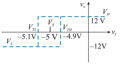
Figure 1
Conclusion:
Therefore, the voltage transfer characteristics are shown in Figure 1.
Want to see more full solutions like this?
Chapter 15 Solutions
Microelectronics: Circuit Analysis and Design


- micro wave.arrow_forwardDon't use ai to answer I will report you answer pleasearrow_forwardDraw the digital modulation outputs, ASK (Amplitude Shift Keying), FSK (Frequency Shift Keying) and PSK (Phase Shift Keying). For baseband and carrier frequency as shown BASESAND 0 CARRIER 101 wwwwwwwwwwwwwarrow_forward
- Don't use ai to answer I will report you answerarrow_forwardplease explain step by step how ti solve these problems and include good explanations. I am most confused with graphing. Thank you, I will give positive feedback. The rest of the questions to this problem are submitted as a new questions due to the multiple part limitarrow_forwardDon't use ai to answer I will report you answerarrow_forward
- This is the last two questions of a previous question I just sent. Please show step by step with clear explanations as to what to do for these questions. I am very confused. Thank you, I will give positive feedbackarrow_forwardNO AI WILL REJECT(using laplace table only)arrow_forwardNO AI WILL REJECT(using laplace table only)arrow_forward
 Introductory Circuit Analysis (13th Edition)Electrical EngineeringISBN:9780133923605Author:Robert L. BoylestadPublisher:PEARSON
 Delmar's Standard Textbook Of ElectricityElectrical EngineeringISBN:9781337900348Author:Stephen L. HermanPublisher:Cengage Learning
 Programmable Logic ControllersElectrical EngineeringISBN:9780073373843Author:Frank D. PetruzellaPublisher:McGraw-Hill Education
 Fundamentals of Electric CircuitsElectrical EngineeringISBN:9780078028229Author:Charles K Alexander, Matthew SadikuPublisher:McGraw-Hill Education
 Electric Circuits. (11th Edition)Electrical EngineeringISBN:9780134746968Author:James W. Nilsson, Susan RiedelPublisher:PEARSON
 Engineering ElectromagneticsElectrical EngineeringISBN:9780078028151Author:Hayt, William H. (william Hart), Jr, BUCK, John A.Publisher:Mcgraw-hill Education,