
(a)
Bias currents
(a)
Answer to Problem 15.16EP
The value of current
The value of current
The reference voltage of temperature compensated portion is 3.08 V
Explanation of Solution
Given:
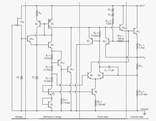
Circuit diagram for voltage regulator is shown below.
The voltage of Zener diode
Transistor parameters of
Also the resistor in the emitter of
The expression for bias current
Substituting 5.6 V for
The value of current
The expression for Emitter-base voltage of transistor
Also,
The expression for emitter-base voltage of transistor
Also,
The expression for emitter-base voltage of transistor
Substituting values of
Substituting value of
Let’s consider the current values 0.205 mA, 0.213 mA, and 0.220 mA for
Substituting values 0.213 mA for
Substituting again 0.220mA for
Hence, the current value 0.213mA is satisfying the equation (2)
After trial and error method it is found that the value of current
The reference voltage of temperature compensated portion (
Substitute 0.6 V for
Hence, the reference voltage of temperature compensated portion is 3.08 V.
(b)
Resistance
(b)
Answer to Problem 15.16EP
The value of resistance
Explanation of Solution
Given:
The voltage of Zener diode
Transistor parameters of
Also the resistor in the emitter of
Given voltage
The expression for reference voltage (
Here,
Let’s re-arrange above expression to find the resistance
Substituting
The value of resistance
Want to see more full solutions like this?
Chapter 15 Solutions
Microelectronics: Circuit Analysis and Design

- What are the benefits of SSBSC modulation compared to DSBFC-AM and DSBSC-AM?arrow_forwardDiscuss the ff. topics in outline form 1.Methods of generating SSB (include the block diagram) Filter method Phase shift method Weaver method 2. Block diagram and difference of Low level modulation and high level modulation 3. Low level modulator: circuit diagram and operation Diode modulator Transistor modulator 4. High level modulator: circuit diagram and operation Collector modulatorarrow_forwarddesign a butterworth 1st order low pass filter . explain and calculate its Voarrow_forward
- Draw block diagram /circuit diagram of the ff. FM circuits and discuss the operation. c. RATIO DETECTORarrow_forwardGiven the information below. Your task is to write a program that samples an analog signal a0 as illustrated below using the MSP430’sADC12 device. Answer the following questions. A. What is the maximum and minimum input voltage of the input signal a0?B. What is the duration of one period of the input signal a0 in milliseconds?C. Let us assume that we configure the MSP430’s device to sample analog input a0 with the sampling frequency fsample = 2 KHz. How many samples, M, do we have per one period of the input analog signal? Fill in the following table by determining the first 6 samples and the last (Mth) sample. Assume that our sampling is synchronized with the a0 (i.e., the first sample is taken at the very beginning of an a0 period). Assume reference voltages VR+ = 2.5 V and VR- = 0V. Sample Number t [ms] a0 [V] Sample value [decimal] 1 2 3 4 5 6 M = E. If you know that…arrow_forward7. The advantage of a differential phase-shift keying (DPSK) system is that_____________ is (are) not required.A. carrier synchronizerB. voltage-controlled oscillatorsC. upper and lower sidebandsD. carrier recovery circuitryarrow_forward
- calculate the loop gain voltage for the circuit shown in this image given that the unity gain frequency of the LF157A is 20MHZ and output for 1kHz and 10 MHz.arrow_forwardExplain by block diagram and equations the PLL method of Demodulating FMarrow_forwardanswer all A - Explain the relation of MOSFET input current and input impedance and their effect on the functionality of the device. B- Explain how to increase the efficiency of the solar cells (PV cells) through the integration of antennas. C- List three conditions need to be considered to choose a MOSFET for switching applications.arrow_forward
- Define angle modulation and list its subcategories.arrow_forwardForm an AM DSBFC envelope with a 40V positive maximum voltage and a 10V positive minimum voltage, determine (a) the unmodulated carrier amplitude, (b) the peak change in amplitude of the modulated wave, and (c) coefficient of modulation and percent modulationarrow_forwardFind the output waveform for the multiplexer attached below.arrow_forward
 Introductory Circuit Analysis (13th Edition)Electrical EngineeringISBN:9780133923605Author:Robert L. BoylestadPublisher:PEARSON
 Delmar's Standard Textbook Of ElectricityElectrical EngineeringISBN:9781337900348Author:Stephen L. HermanPublisher:Cengage Learning
 Programmable Logic ControllersElectrical EngineeringISBN:9780073373843Author:Frank D. PetruzellaPublisher:McGraw-Hill Education
 Fundamentals of Electric CircuitsElectrical EngineeringISBN:9780078028229Author:Charles K Alexander, Matthew SadikuPublisher:McGraw-Hill Education
 Electric Circuits. (11th Edition)Electrical EngineeringISBN:9780134746968Author:James W. Nilsson, Susan RiedelPublisher:PEARSON
 Engineering ElectromagneticsElectrical EngineeringISBN:9780078028151Author:Hayt, William H. (william Hart), Jr, BUCK, John A.Publisher:Mcgraw-hill Education,