
Concept explainers
Videos
Consider the circuit shown in Figure 1.46. The diode can be either a pn junction diode or a Schottky diode. Assume the cut−in voltages are
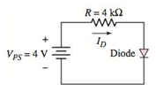
Figure 1.46 Circuit for exercise problem TYU 1.15. The diode can be cither a pn junction diode or a Schottky diode.
Want to see the full answer?
Check out a sample textbook solution
Chapter 1 Solutions
Microelectronics: Circuit Analysis and Design


- Please solve in detailarrow_forward6.7 The transmitting aerial shown in Fig. Q.3 is supplied with current at 80 A peak and at frequency 666.66 kHz. Calculate (a) the effective height of the aerial, and (b) the electric field strength produced at ground level 40 km away. 60 m Fig. Q.3 Input 48 m Eartharrow_forwardox SIM 12.11 Consider the class B output stage, using MOSFETs, shown in Fig. P12.11. Let the devices have |V|= 0.5 V and μC WIL = 2 mA/V². With a 10-kHz sine-wave input of 5-V peak and a high value of load resistance, what peak output would you expect? What fraction of the sine-wave period does the crossover interval represent? For what value of load resistor is the peak output voltage reduced to half the input? Figure P12.11 +5 V Q1 Q2 -5Varrow_forward
- 4 H ་་་་་་་ 四一周 A H₂ Find out put c I writ R as a function G, H, Harrow_forward4 H A H₂ 四一周 Find out put c I writ R as a function G, H, Harrow_forward8. (a) In a Round-Robin tournament, the Tigers beat the Blue Jays, the Tigers beat the Cardinals, the Tigers beat the Orioles, the Blue Jays beat the Cardinals, the Blue Jays beat the Orioles and the Cardinals beat the Orioles. Model this outcome with a directed graph. https://www.akubihar.com (b) (c) ✓ - Let G = (V, E) be a simple graph. Let R be the relation on V consisting of pairs of vertices (u, v) such that there is a path from u to vor such that u= v. Show that R is an equivalence relation. 3 3 Determine whether the following given pair of directed graphs, shown in Fig. 1 and Fig. 2, are isomorphic or not. Exhibit an isomorphism or provide a rigorous argument that none exists. 4+4=8 Աշ աշ ИНИЯ Fig. 1 Fig. 2 Querarrow_forward
- EXAMPLE 4.5 Objective: Determine ID, circuit. V SG' SD Vs and the small - signal voltage gain of a PMOS transistor Consider the circuit shown in Figure 4.20(a). The transistor parameters are A K = 0.80m- V Р _2’TP = 0.5V, and λ = 0 Varrow_forwardNeed a solution and don't use chatgptarrow_forwardNeed a solarrow_forward

 Electricity for Refrigeration, Heating, and Air C...Mechanical EngineeringISBN:9781337399128Author:Russell E. SmithPublisher:Cengage Learning
 Delmar's Standard Textbook Of ElectricityElectrical EngineeringISBN:9781337900348Author:Stephen L. HermanPublisher:Cengage Learning