
Microelectronics: Circuit Analysis and Design
4th Edition
ISBN: 9780073380643
Author: Donald A. Neamen
Publisher: McGraw-Hill Companies, The
expand_more
expand_more
format_list_bulleted
Concept explainers
Videos
Textbook Question
Chapter 1, Problem 1.43P
(a) Consider the circuit shown in Figure P1.40. The value of
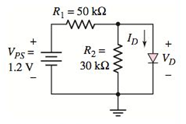
Figure P1.40
Expert Solution & Answer
Want to see the full answer?
Check out a sample textbook solution
Students have asked these similar questions
A practical silicon-based solar cell is constructed from a n+p junction.
a) Explain briefly the meaning of the notation n+?
b) Draw a sketch showing the device structure of this solar cell.
c) This cell shows a photocurrent IL = 10.9 A under AM1.5G illumination.
If the temperature is 25 oC, what is VOC? Assume that the saturated current IS = 1×10⁻⁹ A.
DEVELOP AND JUSTIFY YOUR RESPONSE.
Determine the total current when BT1 = 15.9 V, BT2 = 7.5 V, the Resistance R1 = 1.1 kΩ and the Resistance R2 = 4.4 kΩ, Consider voltage drop of the diodes of Si = 0.7V
A. -2.55 mA.
B. 1,40 mA.
C. 4.25 mA.
D. -1.53 mA.
In the given system; Va, Vb, Vc effective value is 220V, Ly=300 mH and Ry=22 Ohms.It was observed that the yuk current is continuous when the tristorier is triggered for alpha=65 degrees; and D1the average value of the diode current was calculated as ID1 avg = 1.703A.Accordingly, calculate the average value of the current flowing through T3. IT3_ avg=?
Chapter 1 Solutions
Microelectronics: Circuit Analysis and Design
Ch. 1 - Calculate the intrinsic carrier concentration in...Ch. 1 - (a) Calculate the majority and minority carrier...Ch. 1 - Consider ntype GaAs at T=300K doped to a...Ch. 1 - Consider silicon at T=300K . Assume the hole...Ch. 1 - Determine the intrinsic carrier concentration in...Ch. 1 - (a) Consider silicon at T=300K . Assume that...Ch. 1 - Using the results of TYU1.2, determine the drift...Ch. 1 - The electron and hole diffusion coefficients in...Ch. 1 - A sample of silicon at T=300K is doped to...Ch. 1 - (a) Calculate Vbi for a GaAs pn junction at T=300K...
Ch. 1 - A silicon pn junction at T=300K is doped at...Ch. 1 - (a) A silicon pn junction at T=300K has a...Ch. 1 - (a) Determine Vbi for a silicon pn junction at...Ch. 1 - A silicon pn junction diode at T=300K has a...Ch. 1 - Recall that the forwardbias diode voltage...Ch. 1 - Consider the circuit in Figure 1.28. Let VPS=4V ,...Ch. 1 - (a) Consider the circuit shown in Figure 1.28. Let...Ch. 1 - The resistor parameter in the circuit shown in...Ch. 1 - Consider the diode and circuit in Exercise EX 1.8....Ch. 1 - Consider the circuit in Figure 1.28. Let R=4k and...Ch. 1 - The power supply (input) voltage in the circuit of...Ch. 1 - (a) The circuit and diode parameters for the...Ch. 1 - Determine the diffusion conductance of a pn...Ch. 1 - Determine the smallsignal diffusion resistance of...Ch. 1 - The diffusion resistance of a pn junction diode at...Ch. 1 - A pn junction diode and a Schottky diode both have...Ch. 1 - Consider the circuit shown in Figure 1.45....Ch. 1 - Consider the circuit shown in Figure 1.46. The...Ch. 1 - A Zener diode has an equivalent series resistance...Ch. 1 - The resistor in the circuit shown in Figure 1.45...Ch. 1 - Describe an intrinsic semiconductor material. What...Ch. 1 - Describe the concept of an electron and a hole as...Ch. 1 - Describe an extrinsic semiconductor material. What...Ch. 1 - Describe the concepts of drift current and...Ch. 1 - How is a pn junction formed? What is meant by a...Ch. 1 - How is a junction capacitance created in a...Ch. 1 - Write the ideal diode currentvoltage relationship....Ch. 1 - Describe the iteration method of analysis and when...Ch. 1 - Describe the piecewise linear model of a diode and...Ch. 1 - Define a load line in a simple diode circuit.Ch. 1 - Under what conditions is the smallsignal model of...Ch. 1 - Describe the operation of a simple solar cell...Ch. 1 - How do the i characteristics of a Schottky barrier...Ch. 1 - What characteristic of a Zener diode is used in...Ch. 1 - Describe the characteristics of a photodiode and a...Ch. 1 - (a) Calculate the intrinsic carrier concentration...Ch. 1 - (a) The intrinsic carrier concentration in silicon...Ch. 1 - Calculate the intrinsic carrier concentration in...Ch. 1 - (a) Find the concentration of electrons and holes...Ch. 1 - Gallium arsenide is doped with acceptor impurity...Ch. 1 - Silicon is doped with 51016 arsenic atoms/cm3 ....Ch. 1 - (a) Calculate the concentration of electrons and...Ch. 1 - A silicon sample is fabricated such that the hole...Ch. 1 - The electron concentration in silicon at T=300K is...Ch. 1 - (a) A silicon semiconductor material is to be...Ch. 1 - (a) The applied electric field in ptype silicon is...Ch. 1 - A drift current density of 120A/cm2 is established...Ch. 1 - An ntype silicon material has a resistivity of...Ch. 1 - (a) The applied conductivity of a silicon material...Ch. 1 - In GaAs, the mobilities are n=8500cm2/Vs and...Ch. 1 - The electron and hole concentrations in a sample...Ch. 1 - The hole concentration in silicon is given by...Ch. 1 - GaAs is doped to Na=1017cm3 . (a) Calculate no and...Ch. 1 - (a) Determine the builtin potential barrier Vbi in...Ch. 1 - Consider a silicon pn junction. The nregion is...Ch. 1 - The donor concentration in the nregion of a...Ch. 1 - Consider a uniformly doped GaAs pn junction with...Ch. 1 - The zerobiased junction capacitance of a silicon...Ch. 1 - The zerobias capacitance of a silicon pn junction...Ch. 1 - The doping concentrations in a silicon pn junction...Ch. 1 - (a) At what reversebias voltage does the...Ch. 1 - (a) The reversesaturation current of a pn junction...Ch. 1 - (a) The reversesaturation current of a pn junction...Ch. 1 - A silicon pn junction diode has an emission...Ch. 1 - Plot log10ID versus VD over the range 0.1VD0.7V...Ch. 1 - (a) Consider a silicon pn junction diode operating...Ch. 1 - A pn junction diode has IS=2nA . (a) Determine the...Ch. 1 - The reversebias saturation current for a set of...Ch. 1 - A germanium pn junction has a diode current of...Ch. 1 - (a)The reversesaturation current of a gallium...Ch. 1 - The reversesaturation current of a silicon pn...Ch. 1 - A silicon pn junction diode has an applied...Ch. 1 - A pn junction diode is in series with a 1M...Ch. 1 - Consider the diode circuit shown in Figure P1.39....Ch. 1 - The diode in the circuit shown in Figure P1.40 has...Ch. 1 - Prob. 1.41PCh. 1 - (a) The reversesaturation current of each diode in...Ch. 1 - (a) Consider the circuit shown in Figure P1.40....Ch. 1 - Consider the circuit shown in Figure P1.44....Ch. 1 - The cutin voltage of the diode shown in the...Ch. 1 - Find I and VO in each circuit shown in Figure...Ch. 1 - Repeat Problem 1.47 if the reversesaturation...Ch. 1 - (a) In the circuit Shown in Figure P1.49, find the...Ch. 1 - Assume each diode in the circuit shown in Figure...Ch. 1 - (a) Consider a pn junction diode biased at IDQ=1mA...Ch. 1 - Determine the smallsignal diffusion resistancefor...Ch. 1 - The diode in the circuit shown in Figure P1.53 is...Ch. 1 - The forwardbias currents in a pn junction diode...Ch. 1 - A pn junction diode and a Schottky diode have...Ch. 1 - The reversesaturation currents of a Schottky diode...Ch. 1 - Consider the Zener diode circuit shown in Figure...Ch. 1 - (a) The Zener diode in Figure P1.57 is ideal with...Ch. 1 - Consider the Zener diode circuit shown in Figure...Ch. 1 - The Output current of a pn junction diode used as...Ch. 1 - Using the currentvoltage characteristics of the...Ch. 1 - (a) Using the currentvoltage characteristics of...Ch. 1 - Use a computer simulation to generate the ideal...Ch. 1 - Use a computer simulation to find the diode...Ch. 1 - Design a diode circuit to produce the load line...Ch. 1 - Design a circuit to produce the characteristics...Ch. 1 - Design a circuit to produce the characteristics...Ch. 1 - Design a circuit to produce the characteristics...
Knowledge Booster


Learn more about
Need a deep-dive on the concept behind this application? Look no further. Learn more about this topic, electrical-engineering and related others by exploring similar questions and additional content below.Similar questions
- R1 = 1 kohms R2 = 1.4 kohms R3 = 6.8 kohms E = 8V D1: Si, rB = 2 ohms, rR = 215 kohms D2: Si, rB = 7 ohms, rR = 590 kohms Apply each of the diode approximations and determine: a) Current through D1 b) Voltage across D_2 c) Voltage across R_3arrow_forwardConsider the battery-charging circuit shown in Figure 9.25 on page 476, in which vs(t) = 20 sin(200πt) , R = 80 Ω , VB = 12 V and the diode is ideal. a. Sketch the current i(t) to scale versus time. b. Determine the average charging current for the battery.arrow_forwardA practical silicon-based solar cell is constructed from a n+ p junction. a. Explain briefly the meaning of the notation n+ ? b. Draw a sketch showing the device structure of this solar cell. c. This cell shows a photocurrent IL = 10.9 A under AM1.5G illumination.If the temperature is 25oC, what is VOC ? Assume that the saturatedcurrent IS = 1×10⁻⁹ A.arrow_forward
- 4670V = VsR = 200kΩ C = 0.1μF Consider the circuit and parameters illustrated above. If a derating factor of 12% is sugested then calculate, 12) the maximum reverse voltage rating of the diodes; 13) the string efficiency of this arrangement; 14) the maximum difference in leakage current of the diodes; 15) the maximum difference in stored charge of the diodes.arrow_forwardb. Calculate the following about the circuit in Figure 2.1 (If silicon diodes are employed in therectification);i. the peak value of the output voltage considering the drop across each diode, Vpk.ii. the average voltage, Vdc.iii. The current through the load resistor, IL.iv. The current diode, Id.v. The frequency of the output signal, Fout.vi. Calculate the efficiency of the full wave rectifier expressed in percentage.vii. Sketch a graph of the input and output voltage against time.arrow_forwardFor the half-wave rectifier circuit shown, the diode is not ideal and is modeled as an ideal voltage source of value Vf= =0.65V in series with an ideal diode. Vin= 2sin(2π10t) and R= 470Ω. What is the magnitude of the diode current at time t=60mst=60ms? 2- At what time between 0and T/4 seconds is the magnitude of the diode current equal to 2.66mA? Tis the period of Vin Enter your answer in millisecondsarrow_forward
- A full wave bridge rectifier is supplied from 230V, 50Hz and uses a transformer of turns ration 15:1. It uses load resistance of 50 ohms. Calculate load voltage and ripple voltage. Assume ideal diode and transformer. Assume ripple factor equals to 0.482. a.Load Voltage= 13.8 V; Ripple Voltage=6.652 V b.Load Voltage= 15.6 V; Ripple Voltage=7.611 V c.Load Voltage= 21.3 V; Ripple Voltage=8.410 V d.Load Voltage= 25.1 V; Ripple Voltage=10.442 Varrow_forwardGiven R1 = 9 Ohms, R2 = 13 Ohms, what is the current value I? This circuit has Silicon diodes with forward voltage of 0.7V. Round off answer to 2 decimal places.arrow_forwardA constant diffusion current of electrons is established through a silicon semiconductor material. The value of current density is Jn= –0.8 A/cm2. The electron concentration at x=0 is n(0)=1.5x1015 cm–3. The diffusion constant of electrons and holes are 35 and 14 cm2/s, respectively . Determine the hole drift current densityarrow_forward
- In the circuit above, assuming that the diode is made of silicon and exhibits a threshold of 0.6 volts for conduction (forward bias) and no significant resistance and the power source is a DC voltage, what is the current flowing through R1? (V=3.6 volts; R1=10 kΩ; R2=20 kΩ)arrow_forwardQ1 (a) For the given circuit in Figure Q1.1, (i) Describe the diode representation as a switch (ii) Identify the condition of the diode and its equivalent circuit. (iii) Calculate ID, VR1, VR2 and Vo with the diode represent as a switch. (iv) Perform the same calculation as (ii) for GaAs diode.arrow_forwarda) determine I1, I2, I3, I4 using 2nd approximation b) determine ID1, ID2, ID3 using 3rd approximation c) determine VR1, VR2, VR3, VR4 using practical diodesarrow_forward
arrow_back_ios
SEE MORE QUESTIONS
arrow_forward_ios
Recommended textbooks for you
 Introductory Circuit Analysis (13th Edition)Electrical EngineeringISBN:9780133923605Author:Robert L. BoylestadPublisher:PEARSON
 Delmar's Standard Textbook Of ElectricityElectrical EngineeringISBN:9781337900348Author:Stephen L. HermanPublisher:Cengage Learning
 Programmable Logic ControllersElectrical EngineeringISBN:9780073373843Author:Frank D. PetruzellaPublisher:McGraw-Hill Education
 Fundamentals of Electric CircuitsElectrical EngineeringISBN:9780078028229Author:Charles K Alexander, Matthew SadikuPublisher:McGraw-Hill Education
 Electric Circuits. (11th Edition)Electrical EngineeringISBN:9780134746968Author:James W. Nilsson, Susan RiedelPublisher:PEARSON
 Engineering ElectromagneticsElectrical EngineeringISBN:9780078028151Author:Hayt, William H. (william Hart), Jr, BUCK, John A.Publisher:Mcgraw-hill Education,
Introductory Circuit Analysis (13th Edition)
Electrical Engineering
ISBN:9780133923605
Author:Robert L. Boylestad
Publisher:PEARSON
Delmar's Standard Textbook Of Electricity
Electrical Engineering
ISBN:9781337900348
Author:Stephen L. Herman
Publisher:Cengage Learning
Programmable Logic Controllers
Electrical Engineering
ISBN:9780073373843
Author:Frank D. Petruzella
Publisher:McGraw-Hill Education
Fundamentals of Electric Circuits
Electrical Engineering
ISBN:9780078028229
Author:Charles K Alexander, Matthew Sadiku
Publisher:McGraw-Hill Education
Electric Circuits. (11th Edition)
Electrical Engineering
ISBN:9780134746968
Author:James W. Nilsson, Susan Riedel
Publisher:PEARSON
Engineering Electromagnetics
Electrical Engineering
ISBN:9780078028151
Author:Hayt, William H. (william Hart), Jr, BUCK, John A.
Publisher:Mcgraw-hill Education,
Diodes Explained - The basics how diodes work working principle pn junction; Author: The Engineering Mindset;https://www.youtube.com/watch?v=Fwj_d3uO5g8;License: Standard Youtube License