
Microelectronics: Circuit Analysis and Design
4th Edition
ISBN: 9780073380643
Author: Donald A. Neamen
Publisher: McGraw-Hill Companies, The
expand_more
expand_more
format_list_bulleted
Concept explainers
Videos
Textbook Question
Chapter 1, Problem 1.16P
The electron and hole concentrations in a sample of silicon are shown in Figure P1.16. Assume the electron and hole mobilities are the same as in Problem 1.12. Determine the total diffusion current density versus distance x for
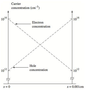
Figure P1.16
Expert Solution & Answer
Want to see the full answer?
Check out a sample textbook solution
Students have asked these similar questions
Consider germanium Ge and GaAs material. Which material has lower intrinsic carrier concentration ni at a fixed temperature and what is the principal reason for that?
Don,t copy from anywhere.Answer follow question step by step.
InP is composed of equal atoms of indium and phosphorus in a lattice similar to that of silicon. (a) Suppose a germanium atom replaces an indium atom in the lattice. Do you expect the germanium atom to behave as a donor or acceptor impurity? Why? (b) Suppose a germanium atom replaces a phosphorus atom in the lattice. Do you expect the germanium atom to behave as a donor or acceptor impurity? Explain.
Please explain temperature dependence of carrier concentration on metals and semiconductors
separately.
Chapter 1 Solutions
Microelectronics: Circuit Analysis and Design
Ch. 1 - Calculate the intrinsic carrier concentration in...Ch. 1 - (a) Calculate the majority and minority carrier...Ch. 1 - Consider ntype GaAs at T=300K doped to a...Ch. 1 - Consider silicon at T=300K . Assume the hole...Ch. 1 - Determine the intrinsic carrier concentration in...Ch. 1 - (a) Consider silicon at T=300K . Assume that...Ch. 1 - Using the results of TYU1.2, determine the drift...Ch. 1 - The electron and hole diffusion coefficients in...Ch. 1 - A sample of silicon at T=300K is doped to...Ch. 1 - (a) Calculate Vbi for a GaAs pn junction at T=300K...
Ch. 1 - A silicon pn junction at T=300K is doped at...Ch. 1 - (a) A silicon pn junction at T=300K has a...Ch. 1 - (a) Determine Vbi for a silicon pn junction at...Ch. 1 - A silicon pn junction diode at T=300K has a...Ch. 1 - Recall that the forwardbias diode voltage...Ch. 1 - Consider the circuit in Figure 1.28. Let VPS=4V ,...Ch. 1 - (a) Consider the circuit shown in Figure 1.28. Let...Ch. 1 - The resistor parameter in the circuit shown in...Ch. 1 - Consider the diode and circuit in Exercise EX 1.8....Ch. 1 - Consider the circuit in Figure 1.28. Let R=4k and...Ch. 1 - The power supply (input) voltage in the circuit of...Ch. 1 - (a) The circuit and diode parameters for the...Ch. 1 - Determine the diffusion conductance of a pn...Ch. 1 - Determine the smallsignal diffusion resistance of...Ch. 1 - The diffusion resistance of a pn junction diode at...Ch. 1 - A pn junction diode and a Schottky diode both have...Ch. 1 - Consider the circuit shown in Figure 1.45....Ch. 1 - Consider the circuit shown in Figure 1.46. The...Ch. 1 - A Zener diode has an equivalent series resistance...Ch. 1 - The resistor in the circuit shown in Figure 1.45...Ch. 1 - Describe an intrinsic semiconductor material. What...Ch. 1 - Describe the concept of an electron and a hole as...Ch. 1 - Describe an extrinsic semiconductor material. What...Ch. 1 - Describe the concepts of drift current and...Ch. 1 - How is a pn junction formed? What is meant by a...Ch. 1 - How is a junction capacitance created in a...Ch. 1 - Write the ideal diode currentvoltage relationship....Ch. 1 - Describe the iteration method of analysis and when...Ch. 1 - Describe the piecewise linear model of a diode and...Ch. 1 - Define a load line in a simple diode circuit.Ch. 1 - Under what conditions is the smallsignal model of...Ch. 1 - Describe the operation of a simple solar cell...Ch. 1 - How do the i characteristics of a Schottky barrier...Ch. 1 - What characteristic of a Zener diode is used in...Ch. 1 - Describe the characteristics of a photodiode and a...Ch. 1 - (a) Calculate the intrinsic carrier concentration...Ch. 1 - (a) The intrinsic carrier concentration in silicon...Ch. 1 - Calculate the intrinsic carrier concentration in...Ch. 1 - (a) Find the concentration of electrons and holes...Ch. 1 - Gallium arsenide is doped with acceptor impurity...Ch. 1 - Silicon is doped with 51016 arsenic atoms/cm3 ....Ch. 1 - (a) Calculate the concentration of electrons and...Ch. 1 - A silicon sample is fabricated such that the hole...Ch. 1 - The electron concentration in silicon at T=300K is...Ch. 1 - (a) A silicon semiconductor material is to be...Ch. 1 - (a) The applied electric field in ptype silicon is...Ch. 1 - A drift current density of 120A/cm2 is established...Ch. 1 - An ntype silicon material has a resistivity of...Ch. 1 - (a) The applied conductivity of a silicon material...Ch. 1 - In GaAs, the mobilities are n=8500cm2/Vs and...Ch. 1 - The electron and hole concentrations in a sample...Ch. 1 - The hole concentration in silicon is given by...Ch. 1 - GaAs is doped to Na=1017cm3 . (a) Calculate no and...Ch. 1 - (a) Determine the builtin potential barrier Vbi in...Ch. 1 - Consider a silicon pn junction. The nregion is...Ch. 1 - The donor concentration in the nregion of a...Ch. 1 - Consider a uniformly doped GaAs pn junction with...Ch. 1 - The zerobiased junction capacitance of a silicon...Ch. 1 - The zerobias capacitance of a silicon pn junction...Ch. 1 - The doping concentrations in a silicon pn junction...Ch. 1 - (a) At what reversebias voltage does the...Ch. 1 - (a) The reversesaturation current of a pn junction...Ch. 1 - (a) The reversesaturation current of a pn junction...Ch. 1 - A silicon pn junction diode has an emission...Ch. 1 - Plot log10ID versus VD over the range 0.1VD0.7V...Ch. 1 - (a) Consider a silicon pn junction diode operating...Ch. 1 - A pn junction diode has IS=2nA . (a) Determine the...Ch. 1 - The reversebias saturation current for a set of...Ch. 1 - A germanium pn junction has a diode current of...Ch. 1 - (a)The reversesaturation current of a gallium...Ch. 1 - The reversesaturation current of a silicon pn...Ch. 1 - A silicon pn junction diode has an applied...Ch. 1 - A pn junction diode is in series with a 1M...Ch. 1 - Consider the diode circuit shown in Figure P1.39....Ch. 1 - The diode in the circuit shown in Figure P1.40 has...Ch. 1 - Prob. 1.41PCh. 1 - (a) The reversesaturation current of each diode in...Ch. 1 - (a) Consider the circuit shown in Figure P1.40....Ch. 1 - Consider the circuit shown in Figure P1.44....Ch. 1 - The cutin voltage of the diode shown in the...Ch. 1 - Find I and VO in each circuit shown in Figure...Ch. 1 - Repeat Problem 1.47 if the reversesaturation...Ch. 1 - (a) In the circuit Shown in Figure P1.49, find the...Ch. 1 - Assume each diode in the circuit shown in Figure...Ch. 1 - (a) Consider a pn junction diode biased at IDQ=1mA...Ch. 1 - Determine the smallsignal diffusion resistancefor...Ch. 1 - The diode in the circuit shown in Figure P1.53 is...Ch. 1 - The forwardbias currents in a pn junction diode...Ch. 1 - A pn junction diode and a Schottky diode have...Ch. 1 - The reversesaturation currents of a Schottky diode...Ch. 1 - Consider the Zener diode circuit shown in Figure...Ch. 1 - (a) The Zener diode in Figure P1.57 is ideal with...Ch. 1 - Consider the Zener diode circuit shown in Figure...Ch. 1 - The Output current of a pn junction diode used as...Ch. 1 - Using the currentvoltage characteristics of the...Ch. 1 - (a) Using the currentvoltage characteristics of...Ch. 1 - Use a computer simulation to generate the ideal...Ch. 1 - Use a computer simulation to find the diode...Ch. 1 - Design a diode circuit to produce the load line...Ch. 1 - Design a circuit to produce the characteristics...Ch. 1 - Design a circuit to produce the characteristics...Ch. 1 - Design a circuit to produce the characteristics...
Knowledge Booster


Learn more about
Need a deep-dive on the concept behind this application? Look no further. Learn more about this topic, electrical-engineering and related others by exploring similar questions and additional content below.Similar questions
- How many valence electrons are generally contained in materials used for insulators?arrow_forwardWe inject electrons into a p-type semiconductor 5 microns long such that the concentration varies linearly from 10E20 cm^-3 to 0 from left to right. If the mobility of the electrons is 500 cm^2/V.s, what is the current density if the electric fields are negligible?arrow_forwardGive/Enumerate other semiconductor materials except Silicon and Germanium? Explain why they are not used in Electronics Devices.arrow_forward
- Explain why Silicon and Germanium are the most common semiconductor materials used in Electronics Devices? Give/Enumerate other semiconductor materials except Silicon and Germanium? Explain why they are not used in Electronics Devices. Explain why Covalent Bonding is used in bonding of semiconductor materials. Explain why Semiconductors are Negative Temperature Coefficient materials?arrow_forwardHow is the surface layer of silicon dioxide formed? how thick is this layer? what are the reasons for forming the Silicon dioxide layer?arrow_forwardThere is a p-type semiconductor box. As the voltage at both ends of the box continued to increase, the drift velocity of the holes in the box reached the saturation velocity. After that, if the acceptor doping concentration in this semiconductor box is doubled and the voltage is also doubled, how will the current change in this semiconductor box change? However, it is assumed that the mobility is affected only by impurity scattering. .arrow_forward
- Indicate a total of 8 factors that determine the breakdown strength in liquid insulators; Explain by drawing the effect of 'electrode shape and opening' expression on breakdown resistance.arrow_forward1) EXPLAIN ELECTRON MOTION IN METAL AND INSULATOR WITH SIMPLE FIGURES? 2) EXPLAIN n-TYPE SEMICONDUCTOR AND DRAW ITS ELECTRONIC BAND STRUCTURE?arrow_forwardDraw band diagrams for below contacts. a) metal-n-type semiconductor for Φm< Φs b) metal-n-type semiconductor for Φm> Φs c) metal-p-type semiconductor for Φm< Φs d) metal-p-type semiconductor for Φm> Φs Clearly specify type of contact, Schottky barrier, built-in-potential and the depletion width in the band diagramarrow_forward
- Q1) a)Explain how doping a pure silicon crystal with donor impurity atoms makes more charge carriers available for conduction.b)Does the above doping result in a p-type or n-type semiconductor? Explain your answer. c) When the diode is forward biased:i) What happens to the barrier potential?ii) What happens to the depletion region?iii) Indicate on your diagram the directions in which the holes and electrons movearrow_forwardQ. Calculate the hole and electron densities in a N-type germaniumsemiconductor at room temperature. The conductivity of semiconductor bar is 500 S/cm. The mobility of electrons and holes at room temperature for germanium is 3800 cm2/ Vs and 1800 cm2/ Vs respectively and ni= 2.5 × 10¹³/cm3.arrow_forwardIn a n-type semiconductor, the electron concentration increases linearly along the x-axis from 10^16 cm^-3 at x=0 (point A) to 5x10^20 cm^-3 at x=0.5cm (point B). In the absence of any external applied electric field, estimate the approximate diffusion current density and its direction (A to B or B to A). Assume that the electron diffusion constant, Dn = 10cm^2/s.arrow_forward
arrow_back_ios
SEE MORE QUESTIONS
arrow_forward_ios
Recommended textbooks for you
 Delmar's Standard Textbook Of ElectricityElectrical EngineeringISBN:9781337900348Author:Stephen L. HermanPublisher:Cengage Learning
Delmar's Standard Textbook Of Electricity
Electrical Engineering
ISBN:9781337900348
Author:Stephen L. Herman
Publisher:Cengage Learning
Diodes Explained - The basics how diodes work working principle pn junction; Author: The Engineering Mindset;https://www.youtube.com/watch?v=Fwj_d3uO5g8;License: Standard Youtube License