
MICROELECT. CIRCUIT ANALYSIS&DESIGN (LL)
4th Edition
ISBN: 9781266368622
Author: NEAMEN
Publisher: MCG
expand_more
expand_more
format_list_bulleted
Concept explainers
Videos
Textbook Question
Chapter 1, Problem 1.44P
Consider the circuit shown in Figure P1.44. Determine the diode current
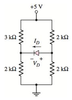
Figure P1.44
Expert Solution & Answer
Want to see the full answer?
Check out a sample textbook solution
Students have asked these similar questions
Consider the circuit shown in Figure 2. The cut-in voltage of each diode is . Let and
assume both diodes are conducting. Determine if this is a valid assumption and
explain your answer. And calculate the values of IR, ID, Ip2, and V..
Rj =1.7 kQ
ww
VB =1 V
D1
Dz
R2D
4 kQ
Figure 2
(I) Determine the average ac resistance for the diode of the Figure below for the region between 0.6 V and 0.9 V. (II) Then determine the ac resistance for the diode of the Figure below at 0.75 V and compare it to the average ac resistance obtained in (I).
2-2VOLTAGE-CURRENT CHARACTERISTICOF A DIODE
1.Explain how to generate the forward-bias portion of the characteristic curve.
2.What would cause the barrier potential of a silicon diode to decrease from 0.7 V to 0.6 V?
Chapter 1 Solutions
MICROELECT. CIRCUIT ANALYSIS&DESIGN (LL)
Ch. 1 - Calculate the intrinsic carrier concentration in...Ch. 1 - (a) Calculate the majority and minority carrier...Ch. 1 - Consider ntype GaAs at T=300K doped to a...Ch. 1 - Consider silicon at T=300K . Assume the hole...Ch. 1 - Determine the intrinsic carrier concentration in...Ch. 1 - (a) Consider silicon at T=300K . Assume that...Ch. 1 - Using the results of TYU1.2, determine the drift...Ch. 1 - The electron and hole diffusion coefficients in...Ch. 1 - A sample of silicon at T=300K is doped to...Ch. 1 - (a) Calculate Vbi for a GaAs pn junction at T=300K...
Ch. 1 - A silicon pn junction at T=300K is doped at...Ch. 1 - (a) A silicon pn junction at T=300K has a...Ch. 1 - (a) Determine Vbi for a silicon pn junction at...Ch. 1 - A silicon pn junction diode at T=300K has a...Ch. 1 - Recall that the forwardbias diode voltage...Ch. 1 - Consider the circuit in Figure 1.28. Let VPS=4V ,...Ch. 1 - (a) Consider the circuit shown in Figure 1.28. Let...Ch. 1 - The resistor parameter in the circuit shown in...Ch. 1 - Consider the diode and circuit in Exercise EX 1.8....Ch. 1 - Consider the circuit in Figure 1.28. Let R=4k and...Ch. 1 - The power supply (input) voltage in the circuit of...Ch. 1 - (a) The circuit and diode parameters for the...Ch. 1 - Determine the diffusion conductance of a pn...Ch. 1 - Determine the smallsignal diffusion resistance of...Ch. 1 - The diffusion resistance of a pn junction diode at...Ch. 1 - A pn junction diode and a Schottky diode both have...Ch. 1 - Consider the circuit shown in Figure 1.45....Ch. 1 - Consider the circuit shown in Figure 1.46. The...Ch. 1 - A Zener diode has an equivalent series resistance...Ch. 1 - The resistor in the circuit shown in Figure 1.45...Ch. 1 - Describe an intrinsic semiconductor material. What...Ch. 1 - Describe the concept of an electron and a hole as...Ch. 1 - Describe an extrinsic semiconductor material. What...Ch. 1 - Describe the concepts of drift current and...Ch. 1 - How is a pn junction formed? What is meant by a...Ch. 1 - How is a junction capacitance created in a...Ch. 1 - Write the ideal diode currentvoltage relationship....Ch. 1 - Describe the iteration method of analysis and when...Ch. 1 - Describe the piecewise linear model of a diode and...Ch. 1 - Define a load line in a simple diode circuit.Ch. 1 - Under what conditions is the smallsignal model of...Ch. 1 - Describe the operation of a simple solar cell...Ch. 1 - How do the i characteristics of a Schottky barrier...Ch. 1 - What characteristic of a Zener diode is used in...Ch. 1 - Describe the characteristics of a photodiode and a...Ch. 1 - (a) Calculate the intrinsic carrier concentration...Ch. 1 - (a) The intrinsic carrier concentration in silicon...Ch. 1 - Calculate the intrinsic carrier concentration in...Ch. 1 - (a) Find the concentration of electrons and holes...Ch. 1 - Gallium arsenide is doped with acceptor impurity...Ch. 1 - Silicon is doped with 51016 arsenic atoms/cm3 ....Ch. 1 - (a) Calculate the concentration of electrons and...Ch. 1 - A silicon sample is fabricated such that the hole...Ch. 1 - The electron concentration in silicon at T=300K is...Ch. 1 - (a) A silicon semiconductor material is to be...Ch. 1 - (a) The applied electric field in ptype silicon is...Ch. 1 - A drift current density of 120A/cm2 is established...Ch. 1 - An ntype silicon material has a resistivity of...Ch. 1 - (a) The applied conductivity of a silicon material...Ch. 1 - In GaAs, the mobilities are n=8500cm2/Vs and...Ch. 1 - The electron and hole concentrations in a sample...Ch. 1 - The hole concentration in silicon is given by...Ch. 1 - GaAs is doped to Na=1017cm3 . (a) Calculate no and...Ch. 1 - (a) Determine the builtin potential barrier Vbi in...Ch. 1 - Consider a silicon pn junction. The nregion is...Ch. 1 - The donor concentration in the nregion of a...Ch. 1 - Consider a uniformly doped GaAs pn junction with...Ch. 1 - The zerobiased junction capacitance of a silicon...Ch. 1 - The zerobias capacitance of a silicon pn junction...Ch. 1 - The doping concentrations in a silicon pn junction...Ch. 1 - (a) At what reversebias voltage does the...Ch. 1 - (a) The reversesaturation current of a pn junction...Ch. 1 - (a) The reversesaturation current of a pn junction...Ch. 1 - A silicon pn junction diode has an emission...Ch. 1 - Plot log10ID versus VD over the range 0.1VD0.7V...Ch. 1 - (a) Consider a silicon pn junction diode operating...Ch. 1 - A pn junction diode has IS=2nA . (a) Determine the...Ch. 1 - The reversebias saturation current for a set of...Ch. 1 - A germanium pn junction has a diode current of...Ch. 1 - (a)The reversesaturation current of a gallium...Ch. 1 - The reversesaturation current of a silicon pn...Ch. 1 - A silicon pn junction diode has an applied...Ch. 1 - A pn junction diode is in series with a 1M...Ch. 1 - Consider the diode circuit shown in Figure P1.39....Ch. 1 - The diode in the circuit shown in Figure P1.40 has...Ch. 1 - Prob. 1.41PCh. 1 - (a) The reversesaturation current of each diode in...Ch. 1 - (a) Consider the circuit shown in Figure P1.40....Ch. 1 - Consider the circuit shown in Figure P1.44....Ch. 1 - The cutin voltage of the diode shown in the...Ch. 1 - Find I and VO in each circuit shown in Figure...Ch. 1 - Repeat Problem 1.47 if the reversesaturation...Ch. 1 - (a) In the circuit Shown in Figure P1.49, find the...Ch. 1 - Assume each diode in the circuit shown in Figure...Ch. 1 - (a) Consider a pn junction diode biased at IDQ=1mA...Ch. 1 - Determine the smallsignal diffusion resistancefor...Ch. 1 - The diode in the circuit shown in Figure P1.53 is...Ch. 1 - The forwardbias currents in a pn junction diode...Ch. 1 - A pn junction diode and a Schottky diode have...Ch. 1 - The reversesaturation currents of a Schottky diode...Ch. 1 - Consider the Zener diode circuit shown in Figure...Ch. 1 - (a) The Zener diode in Figure P1.57 is ideal with...Ch. 1 - Consider the Zener diode circuit shown in Figure...Ch. 1 - The Output current of a pn junction diode used as...Ch. 1 - Using the currentvoltage characteristics of the...Ch. 1 - (a) Using the currentvoltage characteristics of...Ch. 1 - Use a computer simulation to generate the ideal...Ch. 1 - Use a computer simulation to find the diode...Ch. 1 - Design a diode circuit to produce the load line...Ch. 1 - Design a circuit to produce the characteristics...Ch. 1 - Design a circuit to produce the characteristics...Ch. 1 - Design a circuit to produce the characteristics...
Knowledge Booster


Learn more about
Need a deep-dive on the concept behind this application? Look no further. Learn more about this topic, electrical-engineering and related others by exploring similar questions and additional content below.Similar questions
- How is a solid-state diode tested? Explain.arrow_forwardWhat is CEMF?arrow_forwardConsider the circuit in the figure below 4:1 120 V rms ooooo gll reelee D₁ L a. What type of circuit is this? b. What is the total peak secondary voltage? D₂ c. Find the peak voltage across each half of the secondary. d. Sketch the voltage waveform across RL. e. What is the peak current through each diode? f. What is the PIV for each diode? RL 1.0 ΚΩarrow_forward
- Consider a Zener diode in the figure given below where, V1 = 30 V. Determine the Zener current IZ if RZ = 100 Ω.arrow_forwardUSING D1 1N4001G or SILICON DIODE. To sketch the characteristic curve of the diode you need to vary voltages on diode and measure current flowing during forward and reverse bias condition. Fill up the table below using circuit shown and vary battery voltages. Measure voltage and current of diode then sketch the graph. Voltage X axis and Current Y axis. Battery Diode Diode Voltage Current Voltage Battery Diode voltage Voltage 0.1V 0.3V 0.5V 0.7V 1.0V 2.0V 3.0V 10.0V Diode Current Forward Bias Condition A V 0.1V 0.5V 2.0V 5.0V 10v 20V 25V 30V Reverse Bias Condition Note: used any electronics software to perform this activityarrow_forwardFigure 2 shows a circuit for charging a 12 v battery. If Vs is a sinusoidal input with 30 v peak amplitude, determine: i. The fraction of each cycle during which the diode conducts. ii. The peak value of the diode current iii. The maximum reverse bias voltage that appears across the di ode. 100 n 12 V Figure 2arrow_forward
- Q1: Draw the current-voltage characteristic of silicon diode? And then explain the behavior of diode according to this characteristic.arrow_forwardConsider the diode circuit shown in Figure P1.39. The diode reversesaturation current is IS = (10^−12) A. Determine the diode current ID anddiode voltage VD. I attached the wrong picture in the last question. Also can you answer with all steps thanks.arrow_forwardQuestion-1: Consider the circuit in Figure below. 1. What type of circuit is this? 2. What is the total peak secondary voltage? B. Find the peak voltage across each half of the secondary. 4. Sketch the output voltage waveform across R1. 5. Sketch the voltage through D1? 6. What is the PIV for each diode? 120 V rms D2arrow_forward
- Q1 Assume that each diode has a turn-on voltage 0.7V in the circuit shown in Figure Q1. By using the constant voltage drop model: 1kN D1 D2 2kN 4k2 6V 3V 4V Figure Q1 a) Show that it is not possible that D1 is on and D2 is off. (Hint: show a contradiction) b) Show that both D1 and D2 are on.arrow_forwardDraw the input waveform and output waveform for the circuit given below with proper values marked in the figure. Assume D1 as germanium and D2 as silicon diodes. Input Vpp%3D20V, V1=3 V and V2=10 V. R D2 D1 Vin Vout V1 V2 Maximum voltage of output waveform Minimum voltage of output waveform Psarrow_forwardDetermine the Q-points for the diode in the circuit given below using the constant voltage drop model with Von = 0.7 V, where R1 = 44 kΩ and R2 = 23 kΩ.arrow_forward
arrow_back_ios
SEE MORE QUESTIONS
arrow_forward_ios
Recommended textbooks for you

 Delmar's Standard Textbook Of ElectricityElectrical EngineeringISBN:9781337900348Author:Stephen L. HermanPublisher:Cengage Learning
Delmar's Standard Textbook Of Electricity
Electrical Engineering
ISBN:9781337900348
Author:Stephen L. Herman
Publisher:Cengage Learning
Diodes Explained - The basics how diodes work working principle pn junction; Author: The Engineering Mindset;https://www.youtube.com/watch?v=Fwj_d3uO5g8;License: Standard Youtube License