
Microelectronics: Circuit Analysis and Design
4th Edition
ISBN: 9780073380643
Author: Donald A. Neamen
Publisher: McGraw-Hill Companies, The
expand_more
expand_more
format_list_bulleted
Videos
Textbook Question
Chapter 5, Problem 5.12TYU
Assume
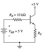
Figure 5.42 Figure for Exercise TYU 5.12
Expert Solution & Answer
Want to see the full answer?
Check out a sample textbook solution
Students have asked these similar questions
Problem5:
For the common base circurt shown in figure find I. and VCB. Assume transistor is
Silicon (a-0.98)
Ic
Rp= 1.5 ko
Rc= 1.2 kn
VEE = 8 V.
Vcc= 18 V
c. For the circuit shown in Figure, determine lc and VCB. Assume the transistor to be made of Silicon.
Ic
RE=1.6 kn
Rc=1.1 kn
EE=8 V
Vcc= 20 v
Q6:A) A transistor dissipates 50W in an ambient temperature of 60°C.The thermal resistance are
exc-0.5
the junction temperature without a heat sink.
Determine the thermal resistance of the heat sink to avoid the junction exceeding 170°C.
°CW¹,0a-4°CW.Determine
5%
single polver supply
Chapter 5 Solutions
Microelectronics: Circuit Analysis and Design
Ch. 5 - An npn transistor is biased in the forwardactive...Ch. 5 - (a) The common-emitter current gains of two...Ch. 5 - An npn transistor is biased in the forwardactive...Ch. 5 - The emitter current in a pnp transistor biased in...Ch. 5 - The output resistance of a bipolar transistor is...Ch. 5 - Assume that IC=1mA at VCE=1V , and that VBE is...Ch. 5 - The openemitter breakdown voltage is BVCBO=200V ,...Ch. 5 - A particular transistor circuit requires a minimum...Ch. 5 - The circuit elements in Figure 5.20(a) are changed...Ch. 5 - The circuit elements in Figure 5.22(a) are V+=3.3V...
Ch. 5 - (a) Verify the results of Example 5.3 with a...Ch. 5 - Consider the pnp circuit in Figure 5.22(a). Assume...Ch. 5 - In the following exercise problems, assume...Ch. 5 - In the following exercise problems, assume...Ch. 5 - The circuit elements in Figure 5.27(a) are changed...Ch. 5 - Using a PSpice simulation, plot the voltage...Ch. 5 - The parameters of the circuit shown in Figure...Ch. 5 - Design the commonbase circuit shown in Figure 5.33...Ch. 5 - The bias voltages in the circuit shown in Figure...Ch. 5 - The bias voltages in the circuit shown in Figure...Ch. 5 - The circuit elements in Figure 5.36(a) are V+=5V ,...Ch. 5 - For the transistor shown in the circuit of Figure...Ch. 5 - For the circuit shown in Figure 5.41, determine...Ch. 5 - Assume =120 for the transistor in Figure 5.42....Ch. 5 - For the transistor in Figure 5.43, assume =90 ....Ch. 5 - (a) Redesign the LED circuit in Figure 5.45(a)...Ch. 5 - The transistor parameters in the circuit in Figure...Ch. 5 - Redesign the inverter amplifier circuit shown in...Ch. 5 - For the circuit shown in Figure 5.44, assume...Ch. 5 - Consider the circuit shown in Figure 5.51(b)....Ch. 5 - [Note: In the following exercises, assume the BE...Ch. 5 - [Note: In the following exercises, assume the B—E...Ch. 5 - Consider the circuit in Figure 5.54(a), let...Ch. 5 - Prob. 5.16EPCh. 5 - The parameters of the circuit shown in Figure...Ch. 5 - Consider the circuit in Figure 5.54(a). The...Ch. 5 - Consider the circuit shown in Figure 5.58. The...Ch. 5 - In the circuit shown in Figure 5.60, the...Ch. 5 - The parameters of the circuit shown in Figure...Ch. 5 - For Figure 5.59, the circuit parameters are...Ch. 5 - In the circuit shown in Figure 5.61, determine new...Ch. 5 - For the circuit shown in Figure 5.63, the circuit...Ch. 5 - (a) Verily the cascode circuit design in Example...Ch. 5 - Prob. 1RQCh. 5 - Prob. 2RQCh. 5 - Prob. 3RQCh. 5 - Define commonbase current gain and commonemitter...Ch. 5 - Discuss the difference between the ac and dc...Ch. 5 - State the relationships between collector,...Ch. 5 - Define Early voltage and collector output...Ch. 5 - Describe a simple commonemitter circuit with an...Ch. 5 - Prob. 9RQCh. 5 - Prob. 10RQCh. 5 - Prob. 11RQCh. 5 - Describe a bipolar transistor NOR logic circuit.Ch. 5 - Describe how a transistor can be used to amplify a...Ch. 5 - Discuss the advantages of using resistor voltage...Ch. 5 - Prob. 15RQCh. 5 - Prob. 16RQCh. 5 - (a) In a bipolar transistor biased in the...Ch. 5 - (a) A bipolar transistor is biased in the...Ch. 5 - (a) The range of ( for a particular type of...Ch. 5 - (a) A bipolar transistor is biased in the...Ch. 5 - Prob. 5.5PCh. 5 - An npn transistor with =80 is connected in a...Ch. 5 - Prob. 5.7PCh. 5 - A pnp transistor with =60 is connected in a...Ch. 5 - (a) The pnp transistor shown in Figure P5.8 has a...Ch. 5 - An npn transistor has a reverse-saturation current...Ch. 5 - Two pnp transistors, fabricated with the same...Ch. 5 - The collector currents in two transistors, A and...Ch. 5 - Prob. 5.13PCh. 5 - Prob. 5.14PCh. 5 - In a particular circuit application, the minimum...Ch. 5 - A particular transistor circuit design requires a...Ch. 5 - For all the transistors in Figure P5.17, =75 . The...Ch. 5 - The emitter resistor values in the circuits show...Ch. 5 - Consider the two circuits in Figure P5.19. The...Ch. 5 - The current gain for each transistor in the...Ch. 5 - Consider the circuits in Figure P5.21. For each...Ch. 5 - (a) The circuit and transistor parameters for the...Ch. 5 - In the circuits shown in Figure P5.23, the values...Ch. 5 - (a) For the circuit in Figure P5.24, determine VB...Ch. 5 - (a) The bias voltages in the circuit shown in...Ch. 5 - The transistor shown in Figure P5.26 has =120 ....Ch. 5 - The transistor in the circuit shown in Figure...Ch. 5 - In the circuit in Figure P5.27, the constant...Ch. 5 - For the circuit shown in Figure P5.29, if =200 for...Ch. 5 - The circuit shown in Figure P5.30 is to be...Ch. 5 - (a) The bias voltage in the circuit in Figure P5.3...Ch. 5 - The current gain of the transistor in the circuit...Ch. 5 - (a) The current gain of the transistor in Figure...Ch. 5 - (a) The transistor shown in Figure P5.34 has =100...Ch. 5 - Assume =120 for the transistor in the circuit...Ch. 5 - For the circuit shown in Figure P5.27, calculate...Ch. 5 - Consider the commonbase circuit shown in Figure...Ch. 5 - (a) For the transistor in Figure P5.38, =80 ....Ch. 5 - Let =25 for the transistor in the circuit shown in...Ch. 5 - (a) The circuit shown in Figure P5.40 is to be...Ch. 5 - The circuit shown in Figure P5.41 is sometimes...Ch. 5 - The transistor in Figure P5.42 has =120 . (a)...Ch. 5 - The commonemitter current gain of the transistor...Ch. 5 - For the circuit shown in Figure P5.44, plot the...Ch. 5 - The transistor in the circuit shown in Figure...Ch. 5 - Consider the circuit in Figure P5.46. For the...Ch. 5 - The current gain for the transistor in the circuit...Ch. 5 - Consider the amplifier circuit shown in Figure...Ch. 5 - For the transistor in the circuit shown in Figure...Ch. 5 - Reconsider Figure P5.49. The transistor current...Ch. 5 - The current gain of the transistor shown in the...Ch. 5 - For the circuit shown in Figure P5.52, let =125 ....Ch. 5 - Consider the circuit shown in Figure P5.53. (a)...Ch. 5 - (a) Redesign the circuit shown in Figure P5.49...Ch. 5 - Prob. 5.55PCh. 5 - Consider the circuit shown in Figure P5.56. (a)...Ch. 5 - (a) Determine the Q-point values for the circuit...Ch. 5 - (a) Determine the Q-point values for the circuit...Ch. 5 - (a) For the circuit shown in Figure P5.59, design...Ch. 5 - Design a bias-stable circuit in the form of Figure...Ch. 5 - Using the circuit in Figure P5.61, design a...Ch. 5 - For the circuit shown in Figure P5.61, the bias...Ch. 5 - (a) A bias-stable circuit with the configuration...Ch. 5 - (a) For the circuit shown in Figure P5.64, assume...Ch. 5 - The dc load line and Q-point of the circuit in...Ch. 5 - The range of ß for the transistor in the circuit...Ch. 5 - The nominal Q-point of the circuit in Figure P5.67...Ch. 5 - (a) For the circuit in Figure P5.67, the value of...Ch. 5 - For the circuit in Figure P5.69, let =100 and...Ch. 5 - Prob. 5.70PCh. 5 - Design the circuit in Figure P5.70 to be bias...Ch. 5 - Consider the circuit shown in Figure P5.72. (a)...Ch. 5 - For the circuit in Figure P5.73, let =100 . (a)...Ch. 5 - Prob. D5.74PCh. 5 - (a) Design a fourresistor bias network with the...Ch. 5 - (a) Design a four-resistor bias network with the...Ch. 5 - (a) A fourresistor bias network is to be designed...Ch. 5 - (a) Design a fourresistor bias network with the...Ch. 5 - For each transistor in the circuit in Figure...Ch. 5 - The parameters for each transistor in the circuit...Ch. 5 - The bias voltage in the circuit shown in Figure...Ch. 5 - Consider the circuit shown in Figure P5.82. The...Ch. 5 - (a) For the transistors in the circuit shown in...Ch. 5 - Using a computer simulation, plot VCE versus V1...Ch. 5 - Using a computer simulation, verify the results of...Ch. 5 - Using a computer simulation, verify the results of...Ch. 5 - Consider a commonemitter circuit with the...Ch. 5 - The emitterfollower circuit shown in Figure P5.89...Ch. 5 - The bias voltages for the circuit in Figure...Ch. 5 - The multitransistor circuit in Figure 5.61 is to...
Knowledge Booster


Learn more about
Need a deep-dive on the concept behind this application? Look no further. Learn more about this topic, electrical-engineering and related others by exploring similar questions and additional content below.Similar questions
- 5.47 The current gain for the transistor in the circuit in Figure P5.47 is B = 60. Determine Rg such that Vo = 8.8 V when V, = 5 V and Ic/Ig = 25. Vec-3v v*-9 V V, ww toro Re= 500 a Van LOV Figure PS.47 Figure PS.48arrow_forwardIdentify the source, drain, gate, and bulk terminalsand find the current I in the transistorsAssume VTN = 0.70 Varrow_forwardAll field-effect transistors are unipolar rather than bipolar devices. That is, the main current through them is comprised either of through an N-type semiconductor * ..... .....arrow_forward
- An NPN silicon transistor having a nominal ß of 100 is to be used in a CE configuration with Vcc= 15 V. The Q point is to be Ic = 4mA and VcE = 12V . Now design the circuit diagram.arrow_forward(a) Determine gm for each of the MOSFET transistors for the gain stage shown in Figure 5-74 (p. 254). Assume Vtn = 0.8V, Vtp = -0.8V, VGS1 = ?, VGS2 = ?, kn = 323 uA/V2, and kp = 162 uA/V2 (b) Determine the voltage gain.arrow_forward04:- Design a bias circuit for NPN silicon transistor having a nominal B-100 to be used in voltage divider circuit with Q-point of Ic 10 mA and VCE = 10 V. Use standard valued 5% resistors and draw a schematic diagram of your design. (10 points)arrow_forward
- The reverse saturation current of an NPN transistor in common-base circuit is 12.5 µA. For an emitter current of 2 mA, collector current is 1.97 mA. Determine the current gain and base current. Î Add filearrow_forward7. MOSFET circuit The MOSFET in the circuit below has V, = 1 V and kn = 4 mA/V². a) Is the MOSFET operating in saturation or in the triode region? b) Determine the drain current Ip and Vout: + 5 V 5 k Voutarrow_forwardThe voltage gain of a common collector transistor is....... O equal to 1 O more than 100 O less than 1 O more than 10 *arrow_forward
- Q-3. Find the drain-source voltage, Vos, for the E- MOSFET circuit given below. The device parameters are: Ioss = 4 mA and Vm = 2 V. +15V Rp- 2k 4M R1 + Vps 2M R2arrow_forwardDraw and explain the schematic diagram for the following: Common Base NPN operating in cut-off region Common Emitter PNP operating in the active region Common Collector NPN operating saturation region From the given figure, identify and explain the 1.Type of Transistor 2. Type of Configuration 3. Mode of Operation V3 SV Q2 100A/A Q3 100A/A 7 V4 5V V6 5Varrow_forwardA transistor current is given below. The Zener diode breakdown voltage is 5.3V as shown. Take base to emitter voltage drop to be 0.6V. The value of the current gain ß is ..... 4.7kQ2 0.5mA ↓ 5.3V www 41 + 0.6- www 22092 47092arrow_forward
arrow_back_ios
SEE MORE QUESTIONS
arrow_forward_ios
Recommended textbooks for you
 Introductory Circuit Analysis (13th Edition)Electrical EngineeringISBN:9780133923605Author:Robert L. BoylestadPublisher:PEARSON
 Delmar's Standard Textbook Of ElectricityElectrical EngineeringISBN:9781337900348Author:Stephen L. HermanPublisher:Cengage Learning
 Programmable Logic ControllersElectrical EngineeringISBN:9780073373843Author:Frank D. PetruzellaPublisher:McGraw-Hill Education
 Fundamentals of Electric CircuitsElectrical EngineeringISBN:9780078028229Author:Charles K Alexander, Matthew SadikuPublisher:McGraw-Hill Education
 Electric Circuits. (11th Edition)Electrical EngineeringISBN:9780134746968Author:James W. Nilsson, Susan RiedelPublisher:PEARSON
 Engineering ElectromagneticsElectrical EngineeringISBN:9780078028151Author:Hayt, William H. (william Hart), Jr, BUCK, John A.Publisher:Mcgraw-hill Education,
Introductory Circuit Analysis (13th Edition)
Electrical Engineering
ISBN:9780133923605
Author:Robert L. Boylestad
Publisher:PEARSON
Delmar's Standard Textbook Of Electricity
Electrical Engineering
ISBN:9781337900348
Author:Stephen L. Herman
Publisher:Cengage Learning
Programmable Logic Controllers
Electrical Engineering
ISBN:9780073373843
Author:Frank D. Petruzella
Publisher:McGraw-Hill Education
Fundamentals of Electric Circuits
Electrical Engineering
ISBN:9780078028229
Author:Charles K Alexander, Matthew Sadiku
Publisher:McGraw-Hill Education
Electric Circuits. (11th Edition)
Electrical Engineering
ISBN:9780134746968
Author:James W. Nilsson, Susan Riedel
Publisher:PEARSON
Engineering Electromagnetics
Electrical Engineering
ISBN:9780078028151
Author:Hayt, William H. (william Hart), Jr, BUCK, John A.
Publisher:Mcgraw-hill Education,
Diode Logic Gates - OR, NOR, AND, & NAND; Author: The Organic Chemistry Tutor;https://www.youtube.com/watch?v=9lqwSaIDm2g;License: Standard Youtube License