
Microelectronics: Circuit Analysis and Design
4th Edition
ISBN: 9780073380643
Author: Donald A. Neamen
Publisher: McGraw-Hill Companies, The
expand_more
expand_more
format_list_bulleted
Videos
Textbook Question
Chapter 5, Problem 5.26P
The transistor shown in Figure P5.26 has
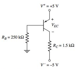
Figure P5.26
Expert Solution & Answer
Want to see the full answer?
Check out a sample textbook solution
Students have asked these similar questions
2.
We discussed in class how the channel capacitance can be modeled in different
region of operations in MOSFETs. For your reference, the slide is shown below.
Explain how you think the model would look like if a transistor is in velocity
saturation region?
Channel Capacitances
Channel capacitance is a voltage dependent and non-linear
capacitance
S
C
P-sub Bulk
Cutoff Region
D
Operation Region
Cutoff
Linear
Saturation
S
P-sub Bulk
C
Linear Region
CGBCH
CoxWLeff
0
0
1
2
3
S
P-sub Bulk
Saturation Region
CGSCH
0
сат
CoxWL eff
1
2
CGDCH
0
CoxWLoft CoxWLoff
eff
D
0
All field-effect transistors are unipolar
rather than bipolar devices. That is, the main
current through them is comprised either of
through an N-type semiconductor *
..... .....
A transistor current is given below. The Zener diode breakdown voltage is 5.3V as
shown. Take base to emitter voltage drop to be 0.6V. The value of the current gain
ß is .....
4.7kQ2
0.5mA ↓
5.3V
www
41
+
0.6-
www
22092
47092
Chapter 5 Solutions
Microelectronics: Circuit Analysis and Design
Ch. 5 - An npn transistor is biased in the forwardactive...Ch. 5 - (a) The common-emitter current gains of two...Ch. 5 - An npn transistor is biased in the forwardactive...Ch. 5 - The emitter current in a pnp transistor biased in...Ch. 5 - The output resistance of a bipolar transistor is...Ch. 5 - Assume that IC=1mA at VCE=1V , and that VBE is...Ch. 5 - The openemitter breakdown voltage is BVCBO=200V ,...Ch. 5 - A particular transistor circuit requires a minimum...Ch. 5 - The circuit elements in Figure 5.20(a) are changed...Ch. 5 - The circuit elements in Figure 5.22(a) are V+=3.3V...
Ch. 5 - (a) Verify the results of Example 5.3 with a...Ch. 5 - Consider the pnp circuit in Figure 5.22(a). Assume...Ch. 5 - In the following exercise problems, assume...Ch. 5 - In the following exercise problems, assume...Ch. 5 - The circuit elements in Figure 5.27(a) are changed...Ch. 5 - Using a PSpice simulation, plot the voltage...Ch. 5 - The parameters of the circuit shown in Figure...Ch. 5 - Design the commonbase circuit shown in Figure 5.33...Ch. 5 - The bias voltages in the circuit shown in Figure...Ch. 5 - The bias voltages in the circuit shown in Figure...Ch. 5 - The circuit elements in Figure 5.36(a) are V+=5V ,...Ch. 5 - For the transistor shown in the circuit of Figure...Ch. 5 - For the circuit shown in Figure 5.41, determine...Ch. 5 - Assume =120 for the transistor in Figure 5.42....Ch. 5 - For the transistor in Figure 5.43, assume =90 ....Ch. 5 - (a) Redesign the LED circuit in Figure 5.45(a)...Ch. 5 - The transistor parameters in the circuit in Figure...Ch. 5 - Redesign the inverter amplifier circuit shown in...Ch. 5 - For the circuit shown in Figure 5.44, assume...Ch. 5 - Consider the circuit shown in Figure 5.51(b)....Ch. 5 - [Note: In the following exercises, assume the BE...Ch. 5 - [Note: In the following exercises, assume the B—E...Ch. 5 - Consider the circuit in Figure 5.54(a), let...Ch. 5 - Prob. 5.16EPCh. 5 - The parameters of the circuit shown in Figure...Ch. 5 - Consider the circuit in Figure 5.54(a). The...Ch. 5 - Consider the circuit shown in Figure 5.58. The...Ch. 5 - In the circuit shown in Figure 5.60, the...Ch. 5 - The parameters of the circuit shown in Figure...Ch. 5 - For Figure 5.59, the circuit parameters are...Ch. 5 - In the circuit shown in Figure 5.61, determine new...Ch. 5 - For the circuit shown in Figure 5.63, the circuit...Ch. 5 - (a) Verily the cascode circuit design in Example...Ch. 5 - Prob. 1RQCh. 5 - Prob. 2RQCh. 5 - Prob. 3RQCh. 5 - Define commonbase current gain and commonemitter...Ch. 5 - Discuss the difference between the ac and dc...Ch. 5 - State the relationships between collector,...Ch. 5 - Define Early voltage and collector output...Ch. 5 - Describe a simple commonemitter circuit with an...Ch. 5 - Prob. 9RQCh. 5 - Prob. 10RQCh. 5 - Prob. 11RQCh. 5 - Describe a bipolar transistor NOR logic circuit.Ch. 5 - Describe how a transistor can be used to amplify a...Ch. 5 - Discuss the advantages of using resistor voltage...Ch. 5 - Prob. 15RQCh. 5 - Prob. 16RQCh. 5 - (a) In a bipolar transistor biased in the...Ch. 5 - (a) A bipolar transistor is biased in the...Ch. 5 - (a) The range of ( for a particular type of...Ch. 5 - (a) A bipolar transistor is biased in the...Ch. 5 - Prob. 5.5PCh. 5 - An npn transistor with =80 is connected in a...Ch. 5 - Prob. 5.7PCh. 5 - A pnp transistor with =60 is connected in a...Ch. 5 - (a) The pnp transistor shown in Figure P5.8 has a...Ch. 5 - An npn transistor has a reverse-saturation current...Ch. 5 - Two pnp transistors, fabricated with the same...Ch. 5 - The collector currents in two transistors, A and...Ch. 5 - Prob. 5.13PCh. 5 - Prob. 5.14PCh. 5 - In a particular circuit application, the minimum...Ch. 5 - A particular transistor circuit design requires a...Ch. 5 - For all the transistors in Figure P5.17, =75 . The...Ch. 5 - The emitter resistor values in the circuits show...Ch. 5 - Consider the two circuits in Figure P5.19. The...Ch. 5 - The current gain for each transistor in the...Ch. 5 - Consider the circuits in Figure P5.21. For each...Ch. 5 - (a) The circuit and transistor parameters for the...Ch. 5 - In the circuits shown in Figure P5.23, the values...Ch. 5 - (a) For the circuit in Figure P5.24, determine VB...Ch. 5 - (a) The bias voltages in the circuit shown in...Ch. 5 - The transistor shown in Figure P5.26 has =120 ....Ch. 5 - The transistor in the circuit shown in Figure...Ch. 5 - In the circuit in Figure P5.27, the constant...Ch. 5 - For the circuit shown in Figure P5.29, if =200 for...Ch. 5 - The circuit shown in Figure P5.30 is to be...Ch. 5 - (a) The bias voltage in the circuit in Figure P5.3...Ch. 5 - The current gain of the transistor in the circuit...Ch. 5 - (a) The current gain of the transistor in Figure...Ch. 5 - (a) The transistor shown in Figure P5.34 has =100...Ch. 5 - Assume =120 for the transistor in the circuit...Ch. 5 - For the circuit shown in Figure P5.27, calculate...Ch. 5 - Consider the commonbase circuit shown in Figure...Ch. 5 - (a) For the transistor in Figure P5.38, =80 ....Ch. 5 - Let =25 for the transistor in the circuit shown in...Ch. 5 - (a) The circuit shown in Figure P5.40 is to be...Ch. 5 - The circuit shown in Figure P5.41 is sometimes...Ch. 5 - The transistor in Figure P5.42 has =120 . (a)...Ch. 5 - The commonemitter current gain of the transistor...Ch. 5 - For the circuit shown in Figure P5.44, plot the...Ch. 5 - The transistor in the circuit shown in Figure...Ch. 5 - Consider the circuit in Figure P5.46. For the...Ch. 5 - The current gain for the transistor in the circuit...Ch. 5 - Consider the amplifier circuit shown in Figure...Ch. 5 - For the transistor in the circuit shown in Figure...Ch. 5 - Reconsider Figure P5.49. The transistor current...Ch. 5 - The current gain of the transistor shown in the...Ch. 5 - For the circuit shown in Figure P5.52, let =125 ....Ch. 5 - Consider the circuit shown in Figure P5.53. (a)...Ch. 5 - (a) Redesign the circuit shown in Figure P5.49...Ch. 5 - Prob. 5.55PCh. 5 - Consider the circuit shown in Figure P5.56. (a)...Ch. 5 - (a) Determine the Q-point values for the circuit...Ch. 5 - (a) Determine the Q-point values for the circuit...Ch. 5 - (a) For the circuit shown in Figure P5.59, design...Ch. 5 - Design a bias-stable circuit in the form of Figure...Ch. 5 - Using the circuit in Figure P5.61, design a...Ch. 5 - For the circuit shown in Figure P5.61, the bias...Ch. 5 - (a) A bias-stable circuit with the configuration...Ch. 5 - (a) For the circuit shown in Figure P5.64, assume...Ch. 5 - The dc load line and Q-point of the circuit in...Ch. 5 - The range of ß for the transistor in the circuit...Ch. 5 - The nominal Q-point of the circuit in Figure P5.67...Ch. 5 - (a) For the circuit in Figure P5.67, the value of...Ch. 5 - For the circuit in Figure P5.69, let =100 and...Ch. 5 - Prob. 5.70PCh. 5 - Design the circuit in Figure P5.70 to be bias...Ch. 5 - Consider the circuit shown in Figure P5.72. (a)...Ch. 5 - For the circuit in Figure P5.73, let =100 . (a)...Ch. 5 - Prob. D5.74PCh. 5 - (a) Design a fourresistor bias network with the...Ch. 5 - (a) Design a four-resistor bias network with the...Ch. 5 - (a) A fourresistor bias network is to be designed...Ch. 5 - (a) Design a fourresistor bias network with the...Ch. 5 - For each transistor in the circuit in Figure...Ch. 5 - The parameters for each transistor in the circuit...Ch. 5 - The bias voltage in the circuit shown in Figure...Ch. 5 - Consider the circuit shown in Figure P5.82. The...Ch. 5 - (a) For the transistors in the circuit shown in...Ch. 5 - Using a computer simulation, plot VCE versus V1...Ch. 5 - Using a computer simulation, verify the results of...Ch. 5 - Using a computer simulation, verify the results of...Ch. 5 - Consider a commonemitter circuit with the...Ch. 5 - The emitterfollower circuit shown in Figure P5.89...Ch. 5 - The bias voltages for the circuit in Figure...Ch. 5 - The multitransistor circuit in Figure 5.61 is to...
Knowledge Booster


Learn more about
Need a deep-dive on the concept behind this application? Look no further. Learn more about this topic, electrical-engineering and related others by exploring similar questions and additional content below.Similar questions
- Q1: for a silicon transistor in the figure below = 200 dc {What is the voltage between the collector and emitter VCE, drawing the load line and finding the Q pointarrow_forwardplease give detail explain.. Ans : Rth = 28 ohm Vth = 92 Varrow_forwardDesign the following MOSFET circuit for it to operate in saturation mode with 0.5 mA drain current. Determine Rp and dc voltage VĎ. Assume V₁ = 2 V and K = 0.1 mA/V² for this MOSFET. 10 V RD -VDarrow_forward
- 04:- Design a bias circuit for NPN silicon transistor having a nominal B-100 to be used in voltage divider circuit with Q-point of Ic 10 mA and VCE = 10 V. Use standard valued 5% resistors and draw a schematic diagram of your design. (10 points)arrow_forwardGive a conclusion about BIPOLAR JUNCTION TRANSISTOR: OPERATION AND ITS CHARACTERISTIC CURVEarrow_forwardPictorially describe the fabrication steps of N-channel E MOSFET. The drawing and steps be in more detailsarrow_forward
- 5.47 The current gain for the transistor in the circuit in Figure P5.47 is B = 60. Determine Rg such that Vo = 8.8 V when V, = 5 V and Ic/Ig = 25. Vec-3v v*-9 V V, ww toro Re= 500 a Van LOV Figure PS.47 Figure PS.48arrow_forwardIn a properly Biased NPN transistor most of the electrons from the emitter A. recombine with holes in the base, B. recombine in the emitter its self, C. pass through the base to the collector, D. are stopped by the junction barrier. In transistor, the relation among emitter current, base current and Collector Current is: A. Ic=IB+IE, B. Ig=IB+Ic, C. IE=Ic-IB, D. I=Ig-Ic. • Transistor is known as bipolar transistor because it has: A. Electrons, В. Holes, C. Electrons and holes, D. None of the above. In NPN or PNP transistor: A. Ic> IE, B. IE >Ic, C. IE = Ic, D. None of the above. The base of an NPN transistor is: A. Heavily doped, B. Lightly doped, C. Medium Doped, D. Doped by pentavalent material. In a transistor the value of a (B) is 100, the value of (a) is: A. 0.01, В. О.1, C. 0.99, D.1.arrow_forwardProblem5: For the common base circurt shown in figure find I. and VCB. Assume transistor is Silicon (a-0.98) Ic Rp= 1.5 ko Rc= 1.2 kn VEE = 8 V. Vcc= 18 Varrow_forward
- For the PN junction under sun light, the short circuit current amount is Isc. Please sketch the I-V curve of PN under the sun based on that under the dark condition above. Indicate Isc and Voc in your plot.arrow_forwarde average voltage of Vo. 5 URM U 2 Figure B.2 shows a circuit using two silicon diodes with knee voltage of 0.7 V. The supply voltage, Vs, is a sinusoidal AC signal. The produced output, Vo, is a fluctuating DC signal with ripple peak-to-peak voltage of I.58 V. & UTM UTM UTM STM DI 5 UTM O UTM 50 Hz &UTM UTM UTM 5 UTM UTM UTM 50 µF RL UTM & UTM D2 &UTM/ UTMTUTM (a) Determine the SITM (b) Determine the peak voltage of the Vs. 5 UTM (c) Consider UTM &UTM & UTM waveform of Vo with complete labelling. en Ci is removed from the circuit (i.e. open circuit). Draw the 5 UTM & UTM UTM U1 A TM 5 UTM UTM TM 5 UTM UTMarrow_forwardAn NPN silicon transistor having a nominal ß of 100 is to be used in a CE configuration with Vcc= 15 V. The Q point is to be Ic = 4mA and VcE = 12V . Now design the circuit diagram.arrow_forward
arrow_back_ios
SEE MORE QUESTIONS
arrow_forward_ios
Recommended textbooks for you
 Introductory Circuit Analysis (13th Edition)Electrical EngineeringISBN:9780133923605Author:Robert L. BoylestadPublisher:PEARSON
 Delmar's Standard Textbook Of ElectricityElectrical EngineeringISBN:9781337900348Author:Stephen L. HermanPublisher:Cengage Learning
 Programmable Logic ControllersElectrical EngineeringISBN:9780073373843Author:Frank D. PetruzellaPublisher:McGraw-Hill Education
 Fundamentals of Electric CircuitsElectrical EngineeringISBN:9780078028229Author:Charles K Alexander, Matthew SadikuPublisher:McGraw-Hill Education
 Electric Circuits. (11th Edition)Electrical EngineeringISBN:9780134746968Author:James W. Nilsson, Susan RiedelPublisher:PEARSON
 Engineering ElectromagneticsElectrical EngineeringISBN:9780078028151Author:Hayt, William H. (william Hart), Jr, BUCK, John A.Publisher:Mcgraw-hill Education,
Introductory Circuit Analysis (13th Edition)
Electrical Engineering
ISBN:9780133923605
Author:Robert L. Boylestad
Publisher:PEARSON
Delmar's Standard Textbook Of Electricity
Electrical Engineering
ISBN:9781337900348
Author:Stephen L. Herman
Publisher:Cengage Learning
Programmable Logic Controllers
Electrical Engineering
ISBN:9780073373843
Author:Frank D. Petruzella
Publisher:McGraw-Hill Education
Fundamentals of Electric Circuits
Electrical Engineering
ISBN:9780078028229
Author:Charles K Alexander, Matthew Sadiku
Publisher:McGraw-Hill Education
Electric Circuits. (11th Edition)
Electrical Engineering
ISBN:9780134746968
Author:James W. Nilsson, Susan Riedel
Publisher:PEARSON
Engineering Electromagnetics
Electrical Engineering
ISBN:9780078028151
Author:Hayt, William H. (william Hart), Jr, BUCK, John A.
Publisher:Mcgraw-hill Education,
How a MOSFET Works - with animation! | Intermediate Electronics; Author: CircuitBread;https://www.youtube.com/watch?v=Bfvyj88Hs_o;License: Standard Youtube License