
Concept explainers
Videos
Consider the circuit shown in Figure 4.28 with circuit parameters VDD=5V , RS=5 kΩ , R1=70.7 kΩ , R2=9.3 kΩ , and RSi=500 Ω . The transistor parameters are: VTP=−0.8V , Kp=0.4 mA/V2 ,and λ=0 . Calculate the small−signal voltage gain Aυ=υo/υi and the output resistance Ro seen looking back into the circuit. (Ans. Aυ=0.817 , Ro=0.915 kΩ )
The values of Av,Ro .
Answer to Problem 4.9EP
Av=0.77Ro=0.914 kΩ
Explanation of Solution
Given Information:
The given circuit is shown below.
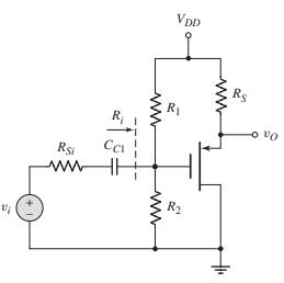
VDD=5 V, RS=5 kΩR1=70.7 kΩ, R2=9.3 kΩRsi=500 Ω, λ=0VTP=−0.8 V, KP=0.4 mAV2
Calculation:
The coupling capacitor acts like open circuit for DC value calculation.
The modified circuit is:
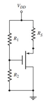
The value of gate voltage is:
VG=R2R1+R2×VDDVG=9.370.7+9.3×5VG=9.3×580VG=0.58 V
From the circuit:
Vs=VDD−IDRSVs=5−5×10³ID
The value of VSG is:
VSG=VS−VGVSG=5−5×10³ID−0.58VSG=4.42−5×10³ID
Assuming the transistor operates in saturation region:
ID=KP(VSG+VTP)2ID=0.4×10⁻³(4.42−5×10³ID−0.8)2ID=0.4×10⁻³(3.62−5×10³ID)2104ID2−15.48ID+5.24×10−3=0ID=1.048 mA,0.5 mA
The value of VSG is:
VSG=4.42−5×10³IDID=1.048 mA,VSG=4.42−5×103×1.048×10−3VSG=−0.82VSG<|VTP|
Hence, the transistor would be in cutoff mode for ID=1.048 mA .
Plugging ID=0.5 mA,
VSG=4.42−5×103×0.5×10−3VSG=1.92 VVSG>|VTP|
The value of VSD is:
VSD=VS−VDVSD=5−5×10³ID−0VSD=5−5×103×0.5×10−3VSD=2.5 V
VSD>VSG+VTP
Hence, the assumption is correct and transistor operates in saturation region.
The DC voltage source and coupling capacitor are short-circuited for small-signal equivalent circuit. It is common drain amplifier.
The modified circuit is:
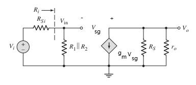
The value of gm,ro is:
gm=2√KPIDgm=2√0.4×10−3×0.5×10−3gm=0.8944 mAVro=1λIDro=10×IDro=∞
The value of output voltage is:
Vo=(−gmVsg)(Rs||ro)Vo=(−gmVsg)Rs ...(1)
Applying Kirchhoff’s voltage law from input to output:
Vin=−Vsg+VoVin=−Vsg−(gmVsg)(Rs)Vsg=−Vin1+gm(Rs)
Applying voltage division rule in input:
Vin=(R1||R2)Rsi+(R1||R2)Vi
Hence, the value of Vsg is:
Vsg=−(R1||R2)(1+gmRs)(Rsi+(R1||R2))Vi
From equation (1):
Vo=−gm(Rs)−(R1||R2)(1+gmRs)(Rsi+(R1||R2))ViVoVi=gmRs(1+gmRs)(RiRsi+Ri)(Ri=R1||R2)Av=0.8944×51+0.8944×5(8.220.5+8.22)Av=0.77
The value of output resistance is:
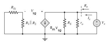
Applying Kirchhoff’s current law at output node:
Ix=gmVsg+VxRs+Vxro
The value of current in input circuit is zero.
Vsg=Vx
Plugging the value:
Ix=gmVx+VxRs+VxroIx=Vx(gm+1Rs+1ro)IxVx=gm+1Rs+1ro1Ro=gm+1Rs+1roRo=1gm||Rs||ro
Plugging the values:
Ro=1gm||Rs||roRo=10.8944||5 (ro=∞)Ro=0.914 kΩ
Want to see more full solutions like this?
Chapter 4 Solutions
Microelectronics: Circuit Analysis and Design


- Choose the best answer for each: 1. What does SRAM use to store data? 。 a) Capacitors ob) Latches 。 c) Flip-flops od) Transistors 2. Which RAM type requires refreshing? o a) SRAM ob) DRAM 。 c) ROM od) Flash 3. What type of memory retains data only while power is on? a) ROM 。 b) EEPROM o c) DRAM od) Flash 4. How many addresses can a 15-bit address bus handle? o a) 32k • b) 64k o c) 16k od) lk 5. What operation occurs when data is copied out of memory without erasing? oa) Write ob) Read o c) Refresh o d) Load 6. DRAM cells store bits using: a) Flip-flops 。 b) Capacitors c) Diodes od) Resistors 7. The cache located inside the CPU is: 。 a) L2 cache o b) LI cache °c) ROM od) HDD 8. SDRAM is synchronized with: o a) Cache ob) Data Bus c) System Clock od) Hard Disk 9. The bus that carries commands is called: o a) Data Bus b) Control Bus o c) Address Bus o d) Logic Bus 10. What is the main use of SRAM? o Disk storage o Cache o Main memory o Registers 11. The smallest addressable unit in…arrow_forwardQ4: A cache memory is 128k × 16. How many bytes can it store?arrow_forwardSketch the output of the analogue computer shown below and find its closest describing function [suppose any variable to find the DF] +1 ew2 HI e2 1.0 +21 LO SJ eo SJ ew LO 1.0 +|e1| HI -1 ew1 ek(1 + e。) |e1| k = 1+|e1| Figure V-5 Feedback Limiter Behavior ROUNDED, DUE TO DIODE NONLINEARITY LIMIT VOLTAGE 409 DIODE CONDUCTS First, write the output transaction, then draw the output wave, and then find the Describing function. I need to solve the question step by step, with an explanation of each step.arrow_forward
- Sketch the output of the analogue computer shown below and find its closest describing function [suppose any variable to find the DF] SJ ew2 ew₁ HI |e2| 2 LO 1.0 +21 LO -1 HI Jel 1.0+|e1| ROUNDED, DUE TO DODE NONLINEARITY LIMIT VOLTAGE DIODE CONDUCTS ew1e, -k(1+ e。) k = |e1| 1+|e1| Figure 1-5 Feedback Limiter Behavior First, write the output transaction, then draw the output wave, and then find the Describing function. I need to solve the question step by step, with an explanation of each step.arrow_forwardSketch the output of the analogue computer shown below and find its closest describing function [suppose any variable to find the DF] SJ +1 HI LO e2 1.0 +21 ew2 eo SJ ew₁ LO Jel 1.0 +|e1| HI -1 ew1 ek(1+eo) k = |e1| 1+|e1| First, write the output transaction, then draw the output wave, and then find the Describing function. I need to solve the question step by step, with an explanation of each step.arrow_forwardCan you help me find the result of an integral 0/2 a² X + a dxarrow_forward
- Q1/Sketch the root locus for the system shown in Figure 1 and find the following: a. The exact point and gain where the locus crosses the jo-axis b. The breakaway point on the real axis c. The range of K within which the system is stable d. Angles of departure and arrival R(s) + K(s²-4s +20) C(s) (s+2)(s + 4)arrow_forwardExam2 Subject: (Numerical Analysis) Class: Third Date: 27/4/2025 Time: 60 minutes Q1. For what values of k does this system of equations has no solution? (use Gauss-Jordan eliminations) kx + y + z = 1 x+ky + z = 1 x+y+kz=1arrow_forwardConsider the Difference equation of a causal Linear time-invariant (LTI) system given by: (y(n) - 1.5y(n - 1) + 0.5y(n = 2) = x(n) a) Implement the difference equation model of this system. b) Find the system transfer function H(z). c) For an input x(n) = 8(n), determine the output response y(n). d) Verify the initial value theorem y(0) with part (c).arrow_forward
- Q5B. Find the type of the controller in the following figures and use real values to find the transfer function of three of them[ Hint Pi,Pd and Lead,lag are found so put the controller with its corresponding compensator]. R₁ R₂ Rz HE C2 RA HE R₁ R2 RA とarrow_forwardQ1// Sketch the root locus for the unity feedback system. Where G(s)=)= K S3+252 +25 and find the following a. Sketch the asymptotes b. The exact point and gain where the locus crosses the jo-axis c. The breakaway point on the real axis d. The range of K within which the system is stable e. Angles of departure and arrival.arrow_forwardDetermine X(w) for the given function shown in Figure (1) by applying the differentiation property of the Fourier Transform. Figure (1) -1 x(t)arrow_forward
 Introductory Circuit Analysis (13th Edition)Electrical EngineeringISBN:9780133923605Author:Robert L. BoylestadPublisher:PEARSON
 Delmar's Standard Textbook Of ElectricityElectrical EngineeringISBN:9781337900348Author:Stephen L. HermanPublisher:Cengage Learning
 Programmable Logic ControllersElectrical EngineeringISBN:9780073373843Author:Frank D. PetruzellaPublisher:McGraw-Hill Education
 Fundamentals of Electric CircuitsElectrical EngineeringISBN:9780078028229Author:Charles K Alexander, Matthew SadikuPublisher:McGraw-Hill Education
 Electric Circuits. (11th Edition)Electrical EngineeringISBN:9780134746968Author:James W. Nilsson, Susan RiedelPublisher:PEARSON
 Engineering ElectromagneticsElectrical EngineeringISBN:9780078028151Author:Hayt, William H. (william Hart), Jr, BUCK, John A.Publisher:Mcgraw-hill Education,