
Videos
Consider the circuit in Figure P4.34. The transistor parameters are
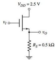
Figure P4.34
Want to see the full answer?
Check out a sample textbook solution
Chapter 4 Solutions
Microelectronics: Circuit Analysis and Design


- QUESTION 4 In this voltage divider bias circuit, the input is at the base. Output is at the emitter with a high input resistance and low output resistance. The maximum voltage gain is 1 and the coupling capacitors must have a negligible reactance at the frequency of operation. (use to answer a and b) a. Derive the expression for the voltage gain, current gain, and power gain in terms of power delivered to the load, RL. b. Sketch both the DC and AC equivalent circuits. c. Derive the expression for ripple factor of Half Wave Rectification with a capacitor filter.arrow_forwardCreate a circuit design that will supply an output voltage of 2VDC, having a 6V DC source supply, using a resistor and a diodes. Current that is flowing on the circuit should be 20mA. It will be used as power source for a small project. (With solution)arrow_forwardQ.3 The input, Vs and the output, Vo of a diode circuit (assuming ideal diode) are shown 3 SEEU/SKEU 1063 in Figure A.2. Name an application that can produce output as in Figure A.2 (ii) and draw the circuit. S UTM S UTM UTM UTM S UTM S UTM O UTM 8 UTM UTM S UTM S UTM UTM UTM S UTM UTM MB UTM ot UTM UT S UTM B UTM UTM 8UTM (i) aUTM UT 8 UTM UTM UTM M UTM TM S UTM UTM UT MS UTM or (i) UTM Figure A.2 8 UTM UT TM S UTMarrow_forward
- b) Figure Q4(b) shows a circuit for voltage to frequency converterarrow_forwarde average voltage of Vo. 5 URM U 2 Figure B.2 shows a circuit using two silicon diodes with knee voltage of 0.7 V. The supply voltage, Vs, is a sinusoidal AC signal. The produced output, Vo, is a fluctuating DC signal with ripple peak-to-peak voltage of I.58 V. & UTM UTM UTM STM DI 5 UTM O UTM 50 Hz &UTM UTM UTM 5 UTM UTM UTM 50 µF RL UTM & UTM D2 &UTM/ UTMTUTM (a) Determine the SITM (b) Determine the peak voltage of the Vs. 5 UTM (c) Consider UTM &UTM & UTM waveform of Vo with complete labelling. en Ci is removed from the circuit (i.e. open circuit). Draw the 5 UTM & UTM UTM U1 A TM 5 UTM UTM TM 5 UTM UTMarrow_forwardUsing a positive Clamper with positive biasing voltage Circuit, with an AC voltage of Vi = 20v with a frequency of 60hz, a value of 500n for the Capacitor, a silicon diode, biased voltage voltage of 5 volts and a resistor with the value of 300 ohms. Find the current on the resistor at a simulation of 20ms in mA. Vm 2Vm R V,m Vo -Vm V, Input Waveform Output Waveform Positive Clamper with positive reference V, wwwarrow_forward
- 2. In the emitter follower discussed in the lectures, the output (emitter) voltage is 0.7V below the input (base) voltage. One way to remove this offset is to use a diode as shown below left. Suppose our input Vi=2V. Assume beta = 100, VCE,SAT=OV, VBE,ON=0.7, and diode Vş=0.7. +5V +5V 1000 R, 500 1N4148 100 Scattering Limit Vo 10 Vio RL=10 R2 -T,= 25 °C 0.1 1K 0.4 0.8 1.2 1.6 2.0 V, - Forward Voltage (V) 94 9170 a. Determine VB and Vo b. Verify your assumed state of the BJT from (a) c. Verify your assumed state of the diode from (a) d. (Optional challenge) To provide good matching between the diode V; and VBE,ON, we need to have at least 1ma passing through Io, as shown in the datasheet figure above right. What is the maximum V, for which Ip is at least 1mA? To increase this limit, should we change R1 or R2 and in what direction (increase or decrease)? 1,- Forward Current (mA)arrow_forwardWhich of the following is a type of Metal Oxide Semiconductor Field Effect Transistor: O P channel JFET O None of them O N channel D- MOSFET in O N channel JFET A simple diode rectifier has 'ripples in the output wave which makes it unsuitable as a DC source. To overcome this one can use of a capacitor in series with a the load resistance. stion Select one: O True O Falsearrow_forwardp4. A biased clamper is connected to a rectangular AC input with 20V on the positive half cycle and -10V on the negative half cycle. The orientation of the Si diode is the same with Vo while the 5V biasing voltage is in opposite connection. The value of R is 100K ohms while the capacitor is 1 microFarad. In P4, what is the voltage across the capacitor? a. 34.3V b. 14.7V c. 24.3V d. 20.7Varrow_forward
- The negative peak value of output waveform for the given circuit diagram is. (VPP of input is 14 V, Bias voltage is 4 V, Diode is silicon) R: D; VN VouTarrow_forward2. In the emitter follower discussed in the lectures, the output (emitter) voltage is 0.7V below the input (base) voltage. One way to remove this offset is to use a diode as shown below left. Suppose our input Vi=2V. Assume beta = 100, VCE,SAT=0V, VBE,ON=0.7, and diode VF=0.7. +5V +5V 1000 R1 1N4148 500 100 Scattering Limit Vo 10 Vi o RL=10 R2 T, = 25 °C 0.1 1K 0 0.4 0.8 1.2 1.6 2.0 V, - Forward Voltage (V) 94 9170 a. Determine VB and V. b. Verify your assumed state of the BJT from (a) c. Verify your assumed state of the diode from (a) d. (Optional challenge) To provide good matching between the diode VF and VBE,ON, we need to have at least 1mA passing through ID, as shown in the datasheet figure above right. What is the maximum V; for which Ip is at least 1mA? To increase this limit, should we change R1 or R2 and in what direction (increase or decrease)? -Forward Current (mA)arrow_forward4.11 For the isolated buck boost converter as shown in the circuit below, the output voltage is to be 35 V at a duty cycle of 30%. The DC input is obtained from a front end rectifier without voltage doubling fed from a 115 V AC. What is the peak forward blocking voltage of the switching element? KH V₁ (a) 232.3 V (c) 162.61 V + ooooo relele S H ww (b) 69.69 V (d) 542 Varrow_forward
 Introductory Circuit Analysis (13th Edition)Electrical EngineeringISBN:9780133923605Author:Robert L. BoylestadPublisher:PEARSON
 Delmar's Standard Textbook Of ElectricityElectrical EngineeringISBN:9781337900348Author:Stephen L. HermanPublisher:Cengage Learning
 Programmable Logic ControllersElectrical EngineeringISBN:9780073373843Author:Frank D. PetruzellaPublisher:McGraw-Hill Education
 Fundamentals of Electric CircuitsElectrical EngineeringISBN:9780078028229Author:Charles K Alexander, Matthew SadikuPublisher:McGraw-Hill Education
 Electric Circuits. (11th Edition)Electrical EngineeringISBN:9780134746968Author:James W. Nilsson, Susan RiedelPublisher:PEARSON
 Engineering ElectromagneticsElectrical EngineeringISBN:9780078028151Author:Hayt, William H. (william Hart), Jr, BUCK, John A.Publisher:Mcgraw-hill Education,