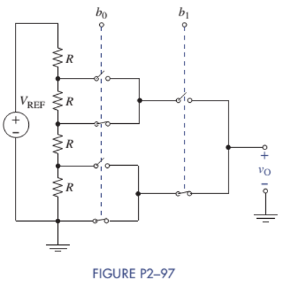
Programmable Voltage Divider Figure P2-97 shows a programmable voltage divider in which digital inputs b 0 and b 1 control complementary analog switches connecting a multitap voltage divider to the analog output vo. The switch positions in the figure apply when digital inputs are low. When inputs go high the switch positions reverse. Find the analog output voltage for ( b 1 , b 0 ) = ( 0 , 0 ) , ( 0 , 1 ) , ( 1 , 0 ) , and ( 1 , 1 ) when V REF = 12 V .
Programmable Voltage Divider Figure P2-97 shows a programmable voltage divider in which digital inputs b 0 and b 1 control complementary analog switches connecting a multitap voltage divider to the analog output vo. The switch positions in the figure apply when digital inputs are low. When inputs go high the switch positions reverse. Find the analog output voltage for ( b 1 , b 0 ) = ( 0 , 0 ) , ( 0 , 1 ) , ( 1 , 0 ) , and ( 1 , 1 ) when V REF = 12 V .
Solution Summary: The author describes the analog output voltage v_O for the given input values. The voltage across each resistor is equal to its resistance divided by the equivalent series resistance.
Figure P2-97 shows a programmable voltage divider in which digital inputs
b
0
and
b
1
control complementary analog switches connecting a multitap voltage divider to the analog output vo. The switch positions in the figure apply when digital inputs are low. When inputs go high the switch positions reverse. Find the analog output voltage for
(
b
1
,
b
0
)
=
(
0
,
0
)
,
(
0
,
1
)
,
(
1
,
0
)
,
and
(
1
,
1
)
when
V
REF
=
12
V
.
The diodes in the circuit in Figure Q7 have V = 0.7.
Determine the output voltage Vo and the currents Ip1,
ID2, D3, and I for the following input conditions:
V₁ = 2V
V₂ = 3V
*** In which all the diodes are ON state
Parameter
Valuc
101 =
6.05 A
D2 =
665 9.05 N
9.65A
03
Vo =
5.725
1 - 10 - 19.50 -0.7 - 5 = 0.45m²ß
U. = 10
19.
H
- (.45mA x 9.5 KR) = 5.725
W
:
5.75 -02:22
0.5. k
IN S. 725-0-7-7
6.05 m/
3
4.0% XIU A
27
2
3
Vo
05 kQ
0.5 k
120 www
IDI
1pz
D₁
D₂
Figure Q7
+10 V
lost [
f
+5 V
9.5 KQ
D
ovo
77°F Clear
For the circuit in figure #2, explain how it works and how JFET works on it.
Determine the gate output for the input waveforms in Figure 3-84 and draw the timing diagram.
0606060
A
B
CH
X
Need a deep-dive on the concept behind this application? Look no further. Learn more about this topic, electrical-engineering and related others by exploring similar questions and additional content below.


 Introductory Circuit Analysis (13th Edition)Electrical EngineeringISBN:9780133923605Author:Robert L. BoylestadPublisher:PEARSON
 Delmar's Standard Textbook Of ElectricityElectrical EngineeringISBN:9781337900348Author:Stephen L. HermanPublisher:Cengage Learning
 Programmable Logic ControllersElectrical EngineeringISBN:9780073373843Author:Frank D. PetruzellaPublisher:McGraw-Hill Education
 Fundamentals of Electric CircuitsElectrical EngineeringISBN:9780078028229Author:Charles K Alexander, Matthew SadikuPublisher:McGraw-Hill Education
 Electric Circuits. (11th Edition)Electrical EngineeringISBN:9780134746968Author:James W. Nilsson, Susan RiedelPublisher:PEARSON
 Engineering ElectromagneticsElectrical EngineeringISBN:9780078028151Author:Hayt, William H. (william Hart), Jr, BUCK, John A.Publisher:Mcgraw-hill Education,