
Videos
(a)
The output voltage
(a)
Answer to Problem 16.3EP
The output voltage
Explanation of Solution
Given:
Power supply voltage,
Intrinsic trans conductance parameter,
Device parameter for driver transistor,
Device parameter for load transistor,
Aspect ratio of driver transistor,
Aspect ratio of load transistor,
When input voltage,
Calculation:
Given depletion-load NMOS inverter:
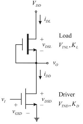
For the NMOS inverter with Depletion load, the output voltage equation is given by
The parameters
Now substituting all the values in the above voltage equation,
On comparing the above equation with quadratic equation
The output voltage cannot be greater than
Conclusion:
Therefore, the output voltage
(b)
The maximum current and maximum power dissipation in the inverter.
(b)
Answer to Problem 16.3EP
The maximum current and maximum power dissipation in the inverter are
Explanation of Solution
Given:
Power supply voltage,
Intrinsic trans conductance parameter,
Device parameter for driver transistor,
Device parameter for load transistor,
Aspect ratio of driver transistor,
Aspect ratio of load transistor,
Calculation:
Maximum current is
Maximum Power dissipated in the inverter is
Conclusion:
Therefore, maximum current and maximum power dissipation in the inverter are
(c)
The transition points for the driver and load transistors.
(c)
Answer to Problem 16.3EP
The transition points for the driver and load transistors are
Explanation of Solution
Given:
Power supply voltage,
Intrinsic trans conductance parameter,
Device parameter for driver transistor,
Device parameter for load transistor,
Aspect ratio of driver transistor,
Aspect ratio of load transistor,
When input voltage,
Calculation:
Transition points for the driver transistor
Output transition point is
Transition points for the load transistor
Output transistor point is
Conclusion:
The transition points for the driver and load transistors are
Want to see more full solutions like this?
Chapter 16 Solutions
MICROELECT. CIRCUIT ANALYSIS&DESIGN (LL)


- A single phase bridge inverter has an RLC load with R= 20 ohms. L = 32 mH and C = 0.115 mF. The inverter frequency is fo= 60 Hz and DC input voltage is Vs = 110 V. The RMS magnitude of the 1st harmonic of the output current is equal to: Select one: a. 4.34A b. 6.42A OC. 0.955A Qd. None of thesearrow_forwardA full-bridge inverter has a switching sequence that produces a square wave voltage across a series RL load. The switching frequency is 60 Hz, Vdc=100 V, R10=Ohm, and L= 25 mH. The power absorbed by the load is. Select one: O a. None of the above O b. 1500 W O c. 1000 W O d. 441 Warrow_forwardA full bridge inverter with RLC load having the following values: R=7.5 Ohms, L=12.5 mH, C=22 uF. The switching frequency is 500 Hz and the DC input voltage is 180V. The THD of the load current is equal to (consider up to the fifth harmonics): Select one: Oa. 8% O b. 12% O c. 6% d. 4%arrow_forward
- The load voltage waveform of a single phase full bridge inverter supplied from 300V DC voltage source is shown in below figure. Output frequency is 50HZ and the load consists of series R-L components. The load values are 22 and 0.04H, respectively. (Conduction interval for half period is 120°) 150 100 50 T -50 3 -100 -150 .002 .004 .006 .008 .01 .012 .014 .016 .018 .02 Time (sec) a. Calculate and draw the load current for the first two-period interval b. Calculate and draw the load current for the steady-state conditionarrow_forwardA single-phase bridge inverter has an RLC load with R20 ohms L-32 mil and C-0115 mF. The inverter frequency is to 60 Hz and DC input voltage is Vs 110 V The phase angle of the load current 5 th harmonics (in degree) is: Select one 0.-28.1 Ob 71.15 ●-71.15 Od 5651 A single phase bridge inverter has an RLC load with R-20 ohm, L32 mit and C-0115 ml The inverter frequency is to 60 Hz and DC input voltage is Vs 110 V The average cument of each transistor is equal to consider up to the fifth hammonies in calculation Select one O None of these OD LEA Oc 223A Od 63A A three phase inverter below has a Y-connected load. The inverter frequency is to 60 Hz and the DC input voltage Vs-220V The applied control signal is a 180 deg conduction mode The RMS Line to Line voltage Vo is equal to Select one O 2425 b. 17963V OC 220N Od. None of thesearrow_forwardOne half bridge inverter with bidirectional switches and one full bridge inverter with bidirectional switches are connected to similar loads (R=102) and providing both an output power of 1 KW. The rms transistor currents of the half bridge and full bridge inverters are respectively: Select one: O a. 5A, 7.07A O b. 5A, 5A O c. 7.07A, 5A Od. None of thesearrow_forward
- A single-phase full bridge inverter is fed for a dc source such that fundamental component of output voltage is 230 V. The input frequency is 50 Hz. Find the rms value of MOSFET and diode currents if load is RLC: R=2 Q, L=19 mH, and C=400 µF. *arrow_forwardThe load voltage waveform of a single phase full bridge inverter supplied from 30OV DC voltage source is shown in below figure. Output frequency is 50HZ and the load consists of series R-L components. The load vahues are 22 and 0.04H, respectively. (Conduction interval for half period is 120°) 150 100 50 T -50 3 -100 -150 .002 .004 .006 008 .01 .012 .014 .016 .018 .02 Time (sec) a. Calculate and draw the load current for the first two-period interval b. Calculate and draw the load current for the steady-state condition c. Find the RMS values of the load voltage and the load current d Calculate and draw the voltage across the load inductance e. Calculate and draw the source current and find its average vahuearrow_forwardThe load voltage waveform of a single phase full bridge inverter supplied from 300V DC voltage source is shown in below figure. Output frequency is 50HZ and the load consists of series R-L components. The load values are 2N and 0.04H, respectively. (Conduction interval for half period is 120°) 150 100 50 T -50 3 -100 -150 .002 .004 .006 .008 .014 ,02 .01 Time (sec) .012 .016 .018 a. Find the RMS values of the load voltage and the load current b. Calculate and draw the voltage across the load inductance c. Calculate and draw the source current and find its average valuearrow_forward
- a) Design a saturated load inverter shown in the figure below with VDD = 3.3 V and VL = 0.25 V. Assume Ipp = 30 µA, K’n = 25 µA/V²' and VIN = 0.65 V. Verify your design using PSPICE or Multisim package. b) Find the noise margins (NML and NMH) associated with the designed inverter graphically and compare them with your calculation. VDD ML HE VSB Msarrow_forwardIn a half bridge inverter with Vs as the supply voltage, the maximum output voltage would be O Vs/4 O vs /2 O Vs 2Vs Ae Lr Ps Pr aarrow_forwardA single phase bridge inverter has an RLC load with R-20 ohm, L32 mit and C-0115 m The inverter frequency is to 60 H and DC input voltage is Vs 110V The average current of each transistor is equal to fontider up to the fifth harmonics in calculation Select on O None of these b 18A Oc 223A Od 6.JAarrow_forward
 Introductory Circuit Analysis (13th Edition)Electrical EngineeringISBN:9780133923605Author:Robert L. BoylestadPublisher:PEARSON
 Delmar's Standard Textbook Of ElectricityElectrical EngineeringISBN:9781337900348Author:Stephen L. HermanPublisher:Cengage Learning
 Programmable Logic ControllersElectrical EngineeringISBN:9780073373843Author:Frank D. PetruzellaPublisher:McGraw-Hill Education
 Fundamentals of Electric CircuitsElectrical EngineeringISBN:9780078028229Author:Charles K Alexander, Matthew SadikuPublisher:McGraw-Hill Education
 Electric Circuits. (11th Edition)Electrical EngineeringISBN:9780134746968Author:James W. Nilsson, Susan RiedelPublisher:PEARSON
 Engineering ElectromagneticsElectrical EngineeringISBN:9780078028151Author:Hayt, William H. (william Hart), Jr, BUCK, John A.Publisher:Mcgraw-hill Education,