
Concept explainers
Videos
(a)
The design parameter for the circuit.
(a)
Answer to Problem D16.11P
The required value of the width to length ratio of the driver is
Explanation of Solution
Calculation:
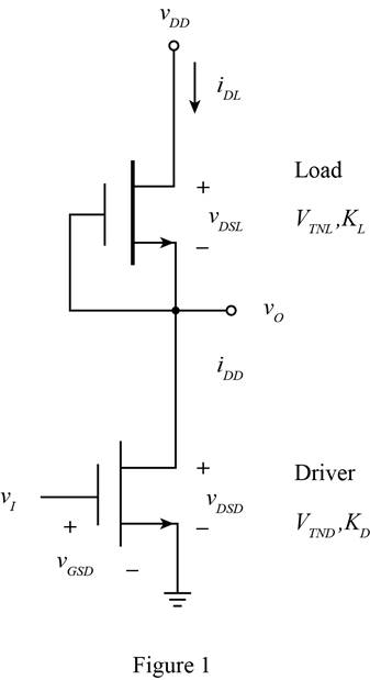
The given diagram is shown in Figure 1
The expression to determine the power dissipated in the circuit is given by,
Substitute
The expression to determine the value of the drain current is given by,
Substitute
The expression to determine the value of the width to length ratio of the driver and the load transistor is given by,
Substitute
The expression for the ratio of the width to length ratio of driver to transistor is given by,
Substitute
Conclusion:
Therefore, the required value of the width to length ratio of the driver is
(b)
The transition for the driver and the load transistor.
(b)
Answer to Problem D16.11P
The value of the input transition point or the load is
Explanation of Solution
Calculation:
For load.
The expression to determine the value of the output transition point is given by,
Substitute
The expression to determine the input transition point is given by,
Substitute
For driver.
The expression to determine the input transition point is given by,
Substitute
The expression to determine the value of the output transition point is given by,
Substitute
Conclusion:
Therefore, the value of the input transition point or the load is
(c)
The value of maximum power dissipation in the inverter and the output voltage for the given input.
(c)
Answer to Problem D16.11P
The value of the output voltage is
Explanation of Solution
Calculation:
The power dissipation is same even if the width to length ratio of the driver is doubled and is given by,
The expression to determine the value of the drain current is given by,
Substitute
The expression for the width to length ratio of the driver is given by,
Substitute
The expression for the ratio of the width to length ratio of driver to transistor is given by,
Substitute
The expression to determine the value of the output voltage is given by,
Substitute
Conclusion:
Therefore, the value of the output voltage is
Want to see more full solutions like this?
Chapter 16 Solutions
MICROELECT. CIRCUIT ANALYSIS&DESIGN (LL)


- A full bridge inverter with RLC load having the following values: R=7.5 Ohms, L=12.5 mH, C=22 uF. The switching frequency is 500 Hz and the DC input voltage is 180V. The THD of the load current is equal to (consider up to the fifth harmonics): Select one: Oa. 8% O b. 12% O c. 6% d. 4%arrow_forwardA single phase bridge inverter has an RLC load with R= 20 ohms. L = 32 mH and C = 0.115 mF. The inverter frequency is fo= 60 Hz and DC input voltage is Vs = 110 V. The RMS magnitude of the 1st harmonic of the output current is equal to: Select one: a. 4.34A b. 6.42A OC. 0.955A Qd. None of thesearrow_forward1. A square-wave inverter has an R-L load with R=15 Ω and L=10 mH. The inverter output frequency is400 Hz (fundamental frequency).(a) Determine the values of the required to establish a load current which has a fundamentalfrequency component of 10 A rms with α = 0.(b) For a controlled full-bridge inverter, the dc source is 125 V and the switching frequency is60 Hz. Determine the value of α to produce an output with amplitude of 100 V at the fundamentalfrequency.arrow_forward
- A full-bridge inverter has a switching sequence that produces a square wave voltage across a series RL load. The switching frequency is 60 Hz, Vdc=100 V, R equals to 10 Ohm, and L equals 25 mH. The average current in the dc source is. Select one: O a. 52 A O b. None of the above O c. 4.41 A O d. 300 Aarrow_forwardThe load voltage waveform of a single phase full bridge inverter supplied from 300V DC voltage source is shown in below figure. Output frequency is 50HZ and the load consists of series R-L components. The load values are 22 and 0.04H, respectively. (Conduction interval for half period is 120°) 150 100 50 T -50 3 -100 -150 .002 .004 .006 .008 .01 .012 .014 .016 .018 .02 Time (sec) a. Calculate and draw the load current for the first two-period interval b. Calculate and draw the load current for the steady-state conditionarrow_forwardUsing the sine PWM method with the full bridge inverter below, it is desired to generate a voltage of 50 Hz on the serial RL load. A voltage of 120 V DC is applied to the input of the inverter circuit. Amplitude modulation rate ma -0.9 and frequency modulation rate mf -19. The resistance of the series RL load is 15 OHM and the coil inductance is 40 mH. a) What is the power drawn by the load resistor?b) What is the total harmonic distortion value (THD) of the load current?arrow_forward
- An inverter with a resistive load, VDD = 3.3 V, P = 0.1 mW, VL = 0.2 V, K'n = 60 UA/V2 and VT N = 0.75 V. The value of (W/L)S is:arrow_forwardThe load voltage waveform of a single phase full bridge inverter supplied from 300V DC voltage source is shown in below figure. Output frequency is 50HZ and the load consists of series R-L components. The load values are 2N and 0.04H, respectively. (Conduction interval for half period is 120°) 150 100 50 T -50 3 -100 -150 .002 .004 .006 .008 .014 ,02 .01 Time (sec) .012 .016 .018 a. Find the RMS values of the load voltage and the load current b. Calculate and draw the voltage across the load inductance c. Calculate and draw the source current and find its average valuearrow_forwardA square-wave inverter has an R-L load with R = 15 N and L = 10 mH. The inverter output frequency is 400 Hz 1. Determine the value of the de source required to establish a load current which has a fundamental frequency component of 10 A rms. (b) Determine the THD of the load current. (c) Sketch the output and input currents. (a)arrow_forward
- 3- In a square wave inverter the switches are controlled in square mode as shown in the bellow. In this inverter V₁ = 100 V and the main frequency of inverter is f = 60 Hz. The load consists of a R = 42 and L= 10 mH. If the main harmonics or this inverter be 1, 3, 5 compute THD voltage and current of load and the effective current of load and power of load and the average current of battery. 10 2.m @t $3,54 VAB Vd -Vd $1,52 N 51 $3 A B İAarrow_forwardA full bridge inverter with RLC load having the following values: R=7.5 Ohms, L=12.5 mH, C-22 uF. The switching frequency is 500 Hz and the DC input voltage is 180V. The average current supply (consider up to the fifth harmonics in calculation) would be equal to: Select one: a. None of these b. 3.84A Ⓒc. 1.64A Ⓒd. 5.74Aarrow_forwardThe following circuit represents an NMOS inverter. Calculate the output voltage V for R= 12,604 n, VoD= 5 V, W/L= 4.3, k,= 34 µA/V, Vx =VGs= 4.93 V, and VT= 0 84 V. Note. Your answer should have tow decimal plačes. VDD VDD Voltage levels in the NMOS inverter. V= V OL Rps (a) NMOS NOT gate W sapproximated by Rps= V2s/lp = 1/ K, (Vos – V7) %3Darrow_forward
 Introductory Circuit Analysis (13th Edition)Electrical EngineeringISBN:9780133923605Author:Robert L. BoylestadPublisher:PEARSON
 Delmar's Standard Textbook Of ElectricityElectrical EngineeringISBN:9781337900348Author:Stephen L. HermanPublisher:Cengage Learning
 Programmable Logic ControllersElectrical EngineeringISBN:9780073373843Author:Frank D. PetruzellaPublisher:McGraw-Hill Education
 Fundamentals of Electric CircuitsElectrical EngineeringISBN:9780078028229Author:Charles K Alexander, Matthew SadikuPublisher:McGraw-Hill Education
 Electric Circuits. (11th Edition)Electrical EngineeringISBN:9780134746968Author:James W. Nilsson, Susan RiedelPublisher:PEARSON
 Engineering ElectromagneticsElectrical EngineeringISBN:9780078028151Author:Hayt, William H. (william Hart), Jr, BUCK, John A.Publisher:Mcgraw-hill Education,