
Concept explainers
Videos
Consider the Schmitt trigger in Figure P15.46. Assume the saturated outputvoltages are
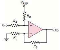
Figure P15.46
(a)
To derive: The expression for the crossover voltage
Answer to Problem 15.46P
The expression for the crossover voltage
Explanation of Solution
Given:
The upper saturated output voltage,
The lowest saturated output voltage,
Calculation:
In an ideal op-amp, the inverting and non-inverting terminal currents are zero. Due to the virtual ground concept, the inverting and non-inverting node voltages are equal.
Given circuit can be represented as
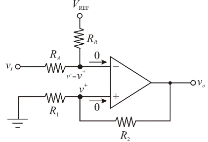
Apply Kirchhoff’s current law at inverting node.
Hence, we get
Apply Kirchhoff’s current law at non-inverting node.
Substitute
When
The upper crossover voltage of Schmitt trigger
Similarly, when
The lower crossover voltage of Schmitt trigger
Conclusion:
Therefore, the expression for the crossover voltage
(b)
To find: the values of
To sketch: The voltage transfer characteristics.
Answer to Problem 15.46P
The required values are
The voltage transfer characteristics are shown in Figure 1
Explanation of Solution
Given:
The circuit voltages are:
Calculation:
The upper crossover voltage is
Therefore, the upper crossover voltage is
The lower crossover voltage is given by,
Therefore, the lower crossover voltage is
The given Schmitt trigger is positive feedback comparator.
Here, the transfer characteristic is a rectangle. Hence, it is called hysteresis which is a dead band. It is so called as the output is not changing
The output remains in the state indefinitely until input voltage crosses the any of the threshold levels.
The voltage transfer characteristics of the given Schmitt trigger is,
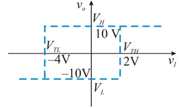
Figure 1
Conclusion:
Therefore, the required values are
Therefore, the voltage transfer characteristics are shown in Figure 1.
Want to see more full solutions like this?
Chapter 15 Solutions
MICROELECT. CIRCUIT ANALYSIS&DESIGN (LL)


- Please do the following, will upvote! Thank you in advance. Do not copy existing chegg answers, I just want gain Kp calculated. A buck converter is to be designed that will convert 42 V input to 12VDC output Calculate the gain Kp required so that the steady state error of the system for a step input is less than 1 % . Assume the triangle wave peak, Vp, has a value of 5 V for your calculations.arrow_forwardHome Work 1/ what js meant by Nyquí st rate ? Q2/ what s meant by Pulse Moduletim ? why we need PM?arrow_forwardQ2. For the circuit shown below, sketch i, & Vo 60 a. Find the conduction angle of the thyristor. b. Find the average output voltage V. R-6.50 f- Go Hz = 27AL = 120x17X10 = 6.4092 075 LO = RrjX= Vo L-17mH 6.5+j6.469=9.128 (44595 075 75V( Es 24 Vm A earrow_forward
- R₁ 22 ΚΩ VIN- R₂ www 220 ΚΩ -VOUT Figure 15.4: A non-inverting amplifier circuit. Consider the op amp circuit in figure 15.4 for the following: 1. If the op amp has a gain bandwidth of 220 kHz, what will the bandwidth of the whole amplifier circuit be?arrow_forward02 1) The PWM is new thechnigue adopted in power electronies application .explaine the advantages of this application 2) In Puls width modulation applieation we Use line and sine wave refrences .explane the advantages and dis advanteges each onearrow_forwardA boost converter has an input voltage Vb=5V. The average load current is lo=0.5A. The switching frequency is 25 kHz. Suppose that a regulator is added (L=0.15 mH and C=0.22 mF) and that the current is continuous. If the average output voltage is Vo =15V, then the ripple current of the inductor delta() is equal to: Select one: a. 1.41A b. 0.56A O c. None of these d. 0.89Aarrow_forward
- For the circuit shown in the figure below, find the output impedance. Assume VÀ < ⁰. Vcc RE Vin KQ₁ - Vout Select one: Rc 7,₁9₂ a. rol // [Rc+ (1/9m2 // roz)] Ob. None of these Oc. ro1 [1+9m1(RE//m1)] // [Rc + (1/9m2 // m2)] O d. rol (1+9m1R) // Rcarrow_forwardWhat type of A/D converter would work best for video signals with a frequency content up to 5 MHz? Why? (Our subject is Principles of Electronic Communications)arrow_forwardDraw a diagram for astable multivibrator using 555 timer. Find the oscillation frequency of the output signal and its duty cycle when the external capacitor is 0.01 uF, the R1 and R2 are 10 kn and 50 kn respectively. While the decoupling capacitor equal 0.1 µF. What happened to the duty cycle when R2 become 1M02?arrow_forward
- 60 fi fs f2 Qs = f = 12,000 Hz the cutoff frequency f2 =.............Hz ▬▬ Q Search book.pat digital-fundamental...arrow_forwardD1 D V1 D4 D2 V D D Diode Model: 1N5817 R = 10k Vi= sine (0 5 100) Given the parameters above, simulate the given circuit using .tran 0 30m 0. Solve for the output peak to peak voltage across the resistor and the output frequency measured across the resistor. Output Frequency = (When computing for the frequency, use 4v as reference point) Output Voltage (pk-pk) = + R1 R D3 Darrow_forwardd) Design (Find the values of the R₁, R2, and C₁) an astable multivibrator circuit to have an output waveform as shown below in the figure (tH = 375µs and t₁ = 125µs). (Assume C₁ = C₂ and R₁ # R₂) and determine the frequency of oscillation and the duty cycle. R1: R2 C1 Q Vcc 4 555 5 C2 10nF I 8 1 3L -OVO tH = 375.0us tL = 125.0usarrow_forward
 Introductory Circuit Analysis (13th Edition)Electrical EngineeringISBN:9780133923605Author:Robert L. BoylestadPublisher:PEARSON
 Delmar's Standard Textbook Of ElectricityElectrical EngineeringISBN:9781337900348Author:Stephen L. HermanPublisher:Cengage Learning
 Programmable Logic ControllersElectrical EngineeringISBN:9780073373843Author:Frank D. PetruzellaPublisher:McGraw-Hill Education
 Fundamentals of Electric CircuitsElectrical EngineeringISBN:9780078028229Author:Charles K Alexander, Matthew SadikuPublisher:McGraw-Hill Education
 Electric Circuits. (11th Edition)Electrical EngineeringISBN:9780134746968Author:James W. Nilsson, Susan RiedelPublisher:PEARSON
 Engineering ElectromagneticsElectrical EngineeringISBN:9780078028151Author:Hayt, William H. (william Hart), Jr, BUCK, John A.Publisher:Mcgraw-hill Education,