
Concept explainers
Videos
(a) Using the small-signal equivalent circuit in Figure 12.25 for the circuit in Figure
(a)
To derive: The expression for the small signal current gain of the circuit.
Answer to Problem 12.50P
The value of the small signal current gain is
Explanation of Solution
Given:
The given circuit is shown in Figure 1.
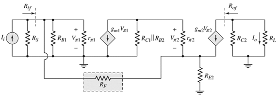
Figure 1
Calculation:
Mark the nodes and redraw the circuit.
The given diagram is shown in Figure 2
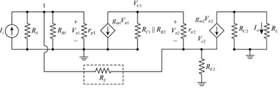
Figure 2
By KCL the expression for the current
The expression for the node voltage is given by,
Apply KCL at node
Substitute
The expression for the output current is given by,
Apply KCL at node
Substitute
Substitute
Consider
Thus, the expression for the small signal current gain is,
Conclusion:
Therefore, the value of the small signal current gain is
(b)
The value of the gain
To compare: The obtained value with the given value of gain. and compare it to the value of 9.58.
Answer to Problem 12.50P
The value of the current gain is
Explanation of Solution
Given:
The given circuit is shown below.

The given value of gain is 9.58.
Also, the values are:
Calculation:
The expression to determine the value of the resistance
The expression for the value of the voltage
The expression to determine the value of the current
Substitute
The value of the current
Substitute
The expression to determine the value of the resistance
The value of the Thevenin voltage is given by,
The expression to determine the value of the current
Substitute
The value of the current
Substitute
The expression to determine the transconductance of first transistor is calculated as,
The expression to determine the transconductance of second transistor is calculated as,
The value of the small signal input resistance is calculated as,
The value of the small signal input resistance is calculated as,
The value of A is calculated as,
The value of B is calculated as,
The value of C is calculated as,
The value of D is calculated as,
Substitute
Substitute
The value of the current gain is
Want to see more full solutions like this?
Chapter 12 Solutions
MICROELECT. CIRCUIT ANALYSIS&DESIGN (LL)


- (b) The multistage amplifier circuit of Figure Q.2(b) have the following parameters: Qı and Q2: B= 200, VBE = 0.7 V, VT = 26 mV , VA=∞ Given that Icọ1 = 2 mA and VCEQ1 = 2 V. (i) Determine the value for R84. List the assumption/approximation made in the analysis. (ii) Sketch and label the small-signal hybrid-t equivalent circuit at midband frequency range. (iii) Calculate the small signal hybrid-n model parameters: gm and ra for Qı and Then, determine Zi2 and Zo. VSI (iv) Find +15 V TU MA RBI 100 k2 UNIVERSITI { Rc 3.3 k2 RB3 10 kN IcQI Q2 C4 Qi VCEQI Ro TEO ► 50 k2 Rs 100 2 RL V. 10k2 RE 2 kN RB4 C3 Zi2 Z, Figure Q.2(b) AYSIAarrow_forwardThis problem is AC analysis problem. DC analysis is not needed to answer the question. A) Convert this bias circuit into a bypassed common emitter amplifier that has an output across a load resistor (RL). To do this you should draw three capacitors on the figure below, an input voltage source, and any resistors you think that should be added. B) In the space below the figure, Draw the hybrid t model for this amplifier circuit including all voltages and resistors. Label Vi, Vbe, and vo on the model. Assume the capacitors you add act as short circuits at AC. Be sure to include resistors R1, R2, R3, R4, and RL in the hybrid pi model. > When you "verify" a mode of operation you will need to calculate all three voltages (Vc, Ve, VE for BJTS and VG, Vs, Vo for MOSFETS) and show the correct two conditions are satisfied. > Assume Capacitors acts like open circuits at DC and short circuits for AC. 12V Assume the following: o Beta = 100 O VBE = 0.7 o V: (Thermal) = 26 mV o Vr (Threshold) = 2V O…arrow_forwardConsider the circuit in Figure 2. The transistor has a parameter B that varies between 50 and 200. You want to know the operation of the circuit and the electrical variables at the end points. Calculate the following for B= 50 and B= 200. a) IE, VE and VB (Analysis in DC). b) The input resistance R." (Small signal analysis). c) The voltage gain VO/Vsing (Small signal analy). This 10 ΚΩ www o Rin 100 ΚΩ +3V +1₁ HH 1 ΚΩ 1₁ 1 ΚΩarrow_forward
- ASAParrow_forwardC. Draw a n-p-n transistor connected in circuit common emitter (CE). Draw the input current-voltage characteristic, the output current-voltage characteristics and the graph giving dependence of the output current as function of the input current. Define the amplification gain of this circuit.arrow_forward1 a) Write down the equation that relates the collector current of the bipolar transistor to the base-emitter voltage. Hence prove the relationship 9mbe Bowhere the ac parameters are transconductance, base-emitter resistance and ac current gain respectively. c) Draw a schematic diagram of a simple current mirror circuit. Show how it can be extended to form a current repeater. How can the current repeater be improved to allow different bias currents to be realised?arrow_forward
- Q3. The transistor parameters in the ac equivalent circuit shown in the figure below are ß1 = B2 = 100, VA1= VA2 =00, Vr= 0.026 v, Icoi = 0.5 mA, and Ico2 = 2 mA. (a) Find the small-signal voltage gain Avi = Vo1/Vi . (b) Determine the small-signal voltage gain Av2 = Vo2/Vo1. (c) Determine the overall small signal voltage gain A,= Vo2/Vị . RE2 C4 k2 Solution: o Vo2 Vol Q2 Rci = 4 k2arrow_forwardWhy is the difference mode gain of circuit given by below?arrow_forwardIn a full-bridge dc-dc converter using PWM bipolar voltage switching, analytically obtain the value of (V/V) which results in the maximum (peak-peak) ripple in the output current i,. Calculate this ripple in terms of Va, La, and farrow_forward
- . To design a bias circuit with an emitter feedback resistor, the voltage from emitter to ground is typically around one-tenth of the supply voltage. true O Falsearrow_forwardFind the following: DC gain, inductor current ripple and output voltage ripple: For DC-DC Buck converter: 1-Draw all circuits in all position 2-Sketch the transistor current waveform 3-Derive analytical expressions for the dc components of the capacitor voltages and inductor currents. 4-Derive analytical expressions for the peak ripple magnitudes of the input filter inductor current and capacitor voltage.arrow_forwardLecturer Karrar Al bayat = Consider the circuit shown in Figure below with transistor parameters ß 120 and VA =00. (a) Determine the small-signal parameters gm, I, and to for both transistors. (b) Plot the dc and ac load lines for both transistors. (c) Determine the overall small-signal voltage gain Av = vo/vs. (d) Determine the input resistance R₁, and the output resistance R.. (e) Determine the maximum Vcc=+12 V undistorted swing in the output voltage. < R₁ = < 67.3 ΚΩ R₂ = Σ 15 ΚΩ Ro R₂ = R₁= 12.7 K 345 ΚΩ Ris Co RC1 = ΤΟ ΚΩ "98 21 REL= <2k2=CE 22 CC3 RE2= RL= 1.6 kΩ < 250 Ω -OUarrow_forward
 Introductory Circuit Analysis (13th Edition)Electrical EngineeringISBN:9780133923605Author:Robert L. BoylestadPublisher:PEARSON
 Delmar's Standard Textbook Of ElectricityElectrical EngineeringISBN:9781337900348Author:Stephen L. HermanPublisher:Cengage Learning
 Programmable Logic ControllersElectrical EngineeringISBN:9780073373843Author:Frank D. PetruzellaPublisher:McGraw-Hill Education
 Fundamentals of Electric CircuitsElectrical EngineeringISBN:9780078028229Author:Charles K Alexander, Matthew SadikuPublisher:McGraw-Hill Education
 Electric Circuits. (11th Edition)Electrical EngineeringISBN:9780134746968Author:James W. Nilsson, Susan RiedelPublisher:PEARSON
 Engineering ElectromagneticsElectrical EngineeringISBN:9780078028151Author:Hayt, William H. (william Hart), Jr, BUCK, John A.Publisher:Mcgraw-hill Education,