
Videos
(a)
The value of the quiescent current
(a)
Answer to Problem 12.46P
The value of
Explanation of Solution
Given:
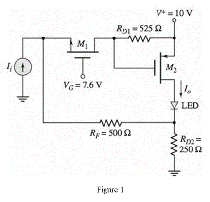
The given diagram is shown in Figure 1

Calculation:
The expression to determine the value of the voltage
The expression for the voltage
The expression for
The expression for the value of the gate to source voltage of the second transistor in terms of the second transistor drain current is given by,
Substitute
Substitute
The expression to determine the value of the gate voltage is given by,
Substitute
From trial and error method the value of the current
The expression for the value of the voltage
Substitute
Substitute
Substitute
Conclusion:
Therefore, the value of
(b)
To show: The expression for the small signal current gain is
(b)
Explanation of Solution
Given:
The given circuit is shown below.
Calculation:
The small signal equivalent circuit is shown in Figure 2
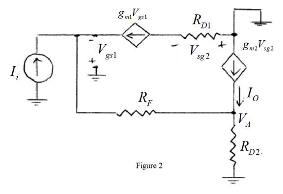
From above the expression for the output current is given by,
The expression for the voltage
Apply KCL at the upper left node.
The expression to determine the value of the
The expression for the value of the current at the output is given by,
Substitute
Substitute
Conclusion:
Therefore, the expression for the current gain is
(c)
The value of the current gain.
(c)
Answer to Problem 12.46P
The value of the current gain is
Explanation of Solution
Given:
The given diagram is shown in Figure 1

Calculation:
The expression to determine the value of the
Substitute
The expression to determine the value of the
Substitute
The expression for the current gain is given by,
Substitute
Conclusion:
Therefore, the value of the current gain is
Want to see more full solutions like this?
Chapter 12 Solutions
MICROELECT. CIRCUIT ANALYSIS&DESIGN (LL)


- The transistor parameters for the circuit in Figure are B, =B2 = 100, VBE1on) = VBE2ton) = 0.7 V, and %3D VA1 =VA2 =0.Find the small signal voltage gain Av = vo/vs. (Note that V-=0.026 V) Vcc=9 V Rib Q1 Vs 1 ko -Ro 20 V 100 Q -wwarrow_forwardc) As given in the figure a clamper circuit with the input signal Vi is proposed to design. Determine the output voltage with the exact solution step by step. Sketch transfer characteristic VO versus Vi.arrow_forwardFind the following: DC gain, inductor current ripple and output voltage ripple: For DC-DC Buck converter: 1-Draw all circuits in all position 2-Sketch the transistor current waveform 3-Derive analytical expressions for the dc components of the capacitor voltages and inductor currents. 4-Derive analytical expressions for the peak ripple magnitudes of the input filter inductor current and capacitor voltage.arrow_forward
- The term duty cycle refers to the amount of time a signal is complete cycle. A. off compared to the period of one B. on The output voltage of op-amp is positive saturation, when the voltage applied to the input is greater than the input. A. inverting B. noninverting A square wave that is 20V at its high state and OV when it is off will produce an average DC when its duty cycle is 75%. Formula: VOUT = Duty Cycle * Peak voltage voltage of A. 7.5V B. 10V C. 15Varrow_forwardC. Draw a n-p-n transistor connected in circuit common emitter (CE). Draw the input current-voltage characteristic, the output current-voltage characteristics and the graph giving dependence of the output current as function of the input current. Define the amplification gain of this circuit.arrow_forwardDraw a n-p-n transistor connected in circuit common base (CB).Draw the input current-voltage characteristic, the output current-voltage characteristicsand the graph giving dependence of the output current as function of the input current.Define the amplification gain of this circuit.arrow_forward
- The saturation current for the de bias circuit with voltage feedback is given by the following: 4. Vcc Rc+ RE Ic = Ic true Falsearrow_forwardA) Design with drawing an Op-Amp series voltage regulator to give a regulated O/P voltage of 12V for an I/P of 15V B) Calculate the line regulation if the I/p increases to 4V leads to increase the O/P voltage to 0.02V.arrow_forwardAmplifier circuit is show below has a single ac input and one ac output. Assuming 2N2222 transistor: Construct the T-model of the transistor with all parameters labelled and evaluated. Assume room temperature. Draw a complete small signal circuit model, then find the voltage gain. Explain two characteristics of this amplifier. Calculate the current gain, the input resistance, and the output resistance.arrow_forward
- Fill in the table VB VC VE Ic LE I8 fre IT gm 5V Consider the circuit given at the right. 600k 1.5k =0.7, Vauo, B=165) 100uF Vo 1k 100uF a) Perform DC analysis and calculate all VB =? VC:? branch currents, node voltages, and small signal parameters 3K VE=? Rout b) Draw a small-signal equivalent model n Vin Rin 400K c) Calculate Ri, Rout, and Ay=Vou/Vin -5Varrow_forwardIt is connected to the input of a transistor (BJT) amplifier circuit with a gain of "-50" with a peak value of 100mV. a sine sign is applied a) Draw the circuit. b) Underline the input and output voltages by specifying their values.arrow_forwardQuestion - qv²= +3 V Rp = 10 k2 = 100 k2 R2 = 200 k2 Rs = 3 k2 (Vt=1V ve Kn=1.0mA/V) (IRF540 N-Channel Mosfet) - Calculate AC parameters. Compute the gain by completing the small signal analysis. Draw the input and output signals to scale.arrow_forward
 Introductory Circuit Analysis (13th Edition)Electrical EngineeringISBN:9780133923605Author:Robert L. BoylestadPublisher:PEARSON
 Delmar's Standard Textbook Of ElectricityElectrical EngineeringISBN:9781337900348Author:Stephen L. HermanPublisher:Cengage Learning
 Programmable Logic ControllersElectrical EngineeringISBN:9780073373843Author:Frank D. PetruzellaPublisher:McGraw-Hill Education
 Fundamentals of Electric CircuitsElectrical EngineeringISBN:9780078028229Author:Charles K Alexander, Matthew SadikuPublisher:McGraw-Hill Education
 Electric Circuits. (11th Edition)Electrical EngineeringISBN:9780134746968Author:James W. Nilsson, Susan RiedelPublisher:PEARSON
 Engineering ElectromagneticsElectrical EngineeringISBN:9780078028151Author:Hayt, William H. (william Hart), Jr, BUCK, John A.Publisher:Mcgraw-hill Education,