
Concept explainers
(a)
The value of resistor R .
(a)
Answer to Problem 10.65P
Explanation of Solution
Given:
Calculation:
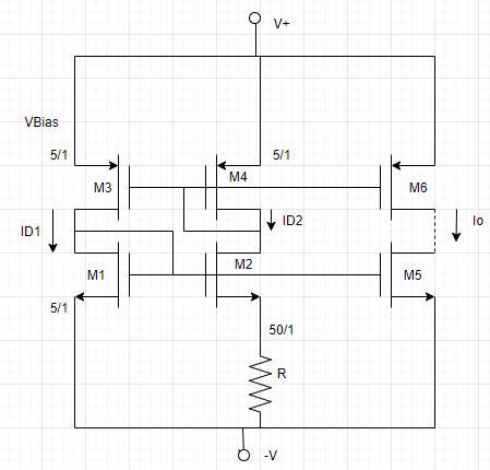
The given circuit is,

According to the statement
Also,
Now calculate R ,
Substitute the given values,
Conclusion:
(b)
The biased voltage difference (
(b)
Answer to Problem 10.65P
Explanation of Solution
Given:
Calculation:
The given circuit is,

According to the circuit,
Now the drain current expression is,
From equation (2),
Now the drain current expression is,
Now from equation (1),
Conclusion:
(c)
The ratio
(c)
Answer to Problem 10.65P
Explanation of Solution
Given:
Calculation:
The given circuit is,
According to the circuit,
Now the drain current expression is,
From equation (2),
Now the drain current expression is,
The expression for current
On substituting the given values,
The expression for current
On substituting the given values,
Conclusion:
Want to see more full solutions like this?
Chapter 10 Solutions
MICROELECT. CIRCUIT ANALYSIS&DESIGN (LL)


- PM BANDWIDTH( NEED NEAT HANDWRITTEN SOLUTION ONLY OTHERWISE DOWNVOTE).arrow_forwardFor circuit shown in the figure with Voc=9 V, Rg=354 kn, Rc=409 0, RE=2.6 kn, B=117, VeE=0.7 V, determine S(lo). Vcc Rc RB Vc |VCE oVE emitter bias configuration Lütfen birini seçin: a.63.38 b.71.86 c.61.96 d.37.75 e.56.97arrow_forwardMake the dc and ac analysis of the circuit below. Vi rms value is given as 2mV. Calculate the value of Vo output signal(rds=50kΩ)arrow_forward
- (a) What are the output currents and output resistances for the current sources as shown if IREF = 45 μA, K'n = 25 μA/V2, VTN = 0.75 V and λ =0.01V−1?(b) What are the currents if IREF is changed to 50 μA?(c) What would be the values if λ =0?arrow_forwardIf the circuit shown in Figure #1 had a 10 kΩ resistor connected as a load resistor, RL and an input signal is applied to the base of the transistor through the coupling capacitor C1, with an amplitude of 22 mVpp at a frequency of 1 kHz. Determine the new voltage gain AV and the output voltage VOUT. Is the output signal clipped?arrow_forwardFor the circuit shown in the figure below, find the output impedance. Assume VÀ < ⁰. Vcc RE Vin KQ₁ - Vout Select one: Rc 7,₁9₂ a. rol // [Rc+ (1/9m2 // roz)] Ob. None of these Oc. ro1 [1+9m1(RE//m1)] // [Rc + (1/9m2 // m2)] O d. rol (1+9m1R) // Rcarrow_forward
- a. Determine the low cutoff frequency for the overall cct. b. Determine the High cutoff frequency for the overall cct c. Sketch approximately the low frequency, and high frequency response for the amplifier overall VI 0.82 ks2 # 0.47 μF 14 V 68 ΚΩ 10 ΚΩ 1.2 ΚΩ Cwi Cwo • 5.6 ΚΩ FIG 9.80 = 5pF Chc= 12 pF = 8 pF Che= 40 pF Cce = 8 pF 0.47 μF HH B = 120 20 μF 13.3 ΚΩarrow_forwardHello! Please show all work, and please show verification for the triodes mode as explained at the bottom, thank you in advance :)arrow_forwardQ2. For the circuit shown below, sketch i, & Vo 60 a. Find the conduction angle of the thyristor. b. Find the average output voltage V. R-6.50 f- Go Hz = 27AL = 120x17X10 = 6.4092 075 LO = RrjX= Vo L-17mH 6.5+j6.469=9.128 (44595 075 75V( Es 24 Vm A earrow_forward
- Please do the following, will upvote! Thank you in advance. Do not copy existing chegg answers, I just want gain Kp calculated. A buck converter is to be designed that will convert 42 V input to 12VDC output Calculate the gain Kp required so that the steady state error of the system for a step input is less than 1 % . Assume the triangle wave peak, Vp, has a value of 5 V for your calculations.arrow_forwardProblem 10. For the following cireuit, a triangular wave E; is applied at the non-inverting terminal and a reference voltage Vrej is applicd at the inverting terminal. [21] +10 V Vref V. Vo E, - 10 V (a) When Vref= 0 V [1] Draw the output waveform Vo and the Vref line: [3] E, (V) Write the name of the circuit below: t (ms) -5 (b) When Vref =+2 V [1] Draw the output waveform Vo and the Vref line: [3] E, (V) Write the name of the circuit below: I (ms) (c) When Vref=-2 V [1] Draw the output waveform Vo and the Vref line: [3] E, (V) Write the name of the circuit below: t (ms)arrow_forwardThe ac equivalent circuit for an amplifier is shown . Assume the capacitors have infinite value, RI = 750 Ω, RB = 100 kΩ, RC = 62 kΩ, and R3 = 100 kΩ. Calculate the voltage gain and input resistance for the amplifier if the BJT Q-point is (40μA, 10 V). Assume βo = 100 and VA = 75V.arrow_forward
 Introductory Circuit Analysis (13th Edition)Electrical EngineeringISBN:9780133923605Author:Robert L. BoylestadPublisher:PEARSON
 Delmar's Standard Textbook Of ElectricityElectrical EngineeringISBN:9781337900348Author:Stephen L. HermanPublisher:Cengage Learning
 Programmable Logic ControllersElectrical EngineeringISBN:9780073373843Author:Frank D. PetruzellaPublisher:McGraw-Hill Education
 Fundamentals of Electric CircuitsElectrical EngineeringISBN:9780078028229Author:Charles K Alexander, Matthew SadikuPublisher:McGraw-Hill Education
 Electric Circuits. (11th Edition)Electrical EngineeringISBN:9780134746968Author:James W. Nilsson, Susan RiedelPublisher:PEARSON
 Engineering ElectromagneticsElectrical EngineeringISBN:9780078028151Author:Hayt, William H. (william Hart), Jr, BUCK, John A.Publisher:Mcgraw-hill Education,