
Videos
The circuit parameters for the two-transistor current source shown inFigure 10.2(b) are
The value of
Answer to Problem 10.1EP
The values are:
Explanation of Solution
Given:
The given circuit is shown below.
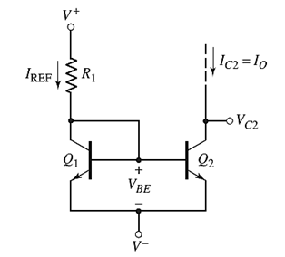
Calculation:
Apply KVL in input Loop
From equation,
From figure,
Also, both transistors are identical (
So,
Want to see more full solutions like this?
Chapter 10 Solutions
MICROELECT. CIRCUIT ANALYSIS&DESIGN (LL)


- Q1. The output characteristic of a typical transistor is shown below, where the quiescent point is selected on it. This transistor is used in the bias circuit presented below. Find the suitable values of Rg and Rc to fix the Q-point of the circuit properly. +Vcc = 12 V 12- Is = 70 uA 10- Ig = 60 uA 8- Rc Is = 50 uA Rs 6- Ig= 40 uA 4. Is = 30 uĄ Is = 20 uA B = 100 2- VBE = 0.7 V 0- -2- 2 4 6 8 10 12 14 16 VCE (V) Ic (mA)arrow_forwardDetermine the ac parameters for this BJT circuit. Note: DC biasing voltages and currents need to be computed FIRST before calculating the AC parameters of gains and impedances 80 mV HI +10 V R₁ 18 ΚΩ R₂ > 4.7 ΚΩ Rc • 1.5 ΚΩ hFE = 30 hfe = 200 RE * 1.2 ΚΩ CE RL > 5.1 ΚΩarrow_forwardFor the circuit shown below, sketch the DC and AC load lines and determine the operating point (Q-point). Vcc +12V R, Rc CH1 10K 2.7K Cout Vout CH2 Cin BC107 2.2µF Vs 2.2µF RE1 R 0.2Vp R2 1202 10K 3.3K f= 10KHZ RE2 CE 1K 10µFarrow_forward
- • Exercise 2: BJT: DC BIASING • For the emitter stabilized bias circuit below, determine BQ, ICQ, VCEQ, VE, Vc and VB and hence draw its DC loadline. Vj o- ⇒C RB 510K Vcc= 22 V Ic Rc = 2K2 C2 R = 1K5 B = 100arrow_forwardGiven the BJT amplifier circuit 18V Rc 3 k2 R1 680 k2 1 µF Io Is R, B=110 Vbe=0.7V 0.6 k 1iF RL ,4.7 k2 VsA RE 0.82k2 Ro' RI' Assume: hfe=ß and hoe is approximately zero. (a) Determine IC and VCE- (b) Determine hie. (c) Determine the equivalent resistances Ri Ri', and Ro'. (d) Determine the current gain Ais=lo/ls. (e) Determine the voltage gai Avs=Vo/Vs. (f) Determine Vo if Vs=200mVp-p.arrow_forwardConsider the circuit shown in figure, where VBE=710 mV, B = 100, and VA = co. Calculate the Vc of Q1. Assume that the emitter current is equal to collector current. al Circuit parameters / Rg = 20 kn, Rc = 300 N, Rɛ = 500 N, Vcc = 3 V Vcc RB Rc REarrow_forward
- In the circuit given in the figure, what is the voltage gain (Av) of the circuit when = 100, r0 = 40 kΩ, RB = 360 kΩ, RC = 3.3 kΩ, RE = 220 Ω, Rs = 15 kΩ and RL = 166 kΩ?NOTE-1: The output impedance r0 of the transistor will be taken into the calculations.NOTE-2: Capacitors are negligible at mid-band frequency.arrow_forwardiv) dc collector to emitter base voltage, VEca v) dc base voltage, VB vi) dc collector voltage, Vc vii) dc emitter voltage, VE and viii) dc base collector voltage, Vsc. ix) ac and dc loadline by using appropriate sketches x) maximum output swing, Vo max. Given : VEB = 0.7V and ß = 100. 12 V 82k 3k3 C. o Vo Vi o H 1k0 39k CE Figure Q3barrow_forwardFor the circult shown in the given figure. Rc-2.4 k0, Rg-10 ko. Pmin-50, and Vcc=5 V. Determine the range of values of Vgg 50 Ic that the transistor is in saturation. Assume Vy-0.6 V and VCEsat -0.2 V. The range of values of VB8 Is VBB> 12 V Ra VAR со Va VCE OE RC Nccarrow_forward
- Given: Voltage Divider Bias Circuit Supply: 10Vdc to 24Vdc Load: 1000 ohms Voltage Gain: 80 to 400 Lower Cutt off Frequency: 100Hz Sinusoidal source (zero internal resistance): 50mVp-p Transistor: Si, beta=75 Base-Collector Capacitance= 8pF Base-Emitter Capacitance= 25pF Design a Single-stage Common Emitter Class A Amplifier and compute the following: a) dc load line b) hie c) midband gain d) Miller equivalent Capacitances e) upper cut off frequencyarrow_forwardThis JFET with the following parameter IDSS = 12mA, Vp = -8V at the following dc bias point (1.) VGS = -0.5V, (2.) VGS = -1.75V, (3.) VGS = -3.5V. Find the a. maximum value of gm (gm0), b. find the value of gm at each operating point. Oarrow_forward5V B OV OV For all the MOSFETS assume Vth=1V and k =50 mA/V² R₁ = 4700 Ao M₁ M₂ B Indicate and verify the state of each MOSFET and Vo for the following input combinations. Fill out the table for each assumed state of the MOSFET for every input combination. Use Rds(on) approximation for linear operation and three significant figures for the voltages. M1 is assumed to be in saturation. If Vgs = 2 V, Vds = 4V, Vds > Vgs - Vth 4>2-1 4> 1 (ok) Vgs > Vth (2>1) A M2 state M3 state V. 0 OV 5 V R₂ = 560Ω 5V M1 state M3arrow_forward
 Introductory Circuit Analysis (13th Edition)Electrical EngineeringISBN:9780133923605Author:Robert L. BoylestadPublisher:PEARSON
 Delmar's Standard Textbook Of ElectricityElectrical EngineeringISBN:9781337900348Author:Stephen L. HermanPublisher:Cengage Learning
 Programmable Logic ControllersElectrical EngineeringISBN:9780073373843Author:Frank D. PetruzellaPublisher:McGraw-Hill Education
 Fundamentals of Electric CircuitsElectrical EngineeringISBN:9780078028229Author:Charles K Alexander, Matthew SadikuPublisher:McGraw-Hill Education
 Electric Circuits. (11th Edition)Electrical EngineeringISBN:9780134746968Author:James W. Nilsson, Susan RiedelPublisher:PEARSON
 Engineering ElectromagneticsElectrical EngineeringISBN:9780078028151Author:Hayt, William H. (william Hart), Jr, BUCK, John A.Publisher:Mcgraw-hill Education,