
(a)
The reference current
(a)
Answer to Problem 10.51P
Explanation of Solution
Given:
The circuit parameters are
The transistor parameters are
Calculation:
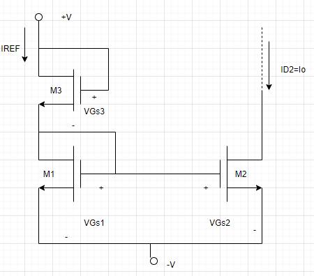
Consider the circuit shown below.

Transistor
Also,
From equation substitute the value of
Also,
The reference current is,
Conclusion:
(b)
The load current
(b)
Answer to Problem 10.51P
Explanation of Solution
Given:
The circuit parameters are
The transistor parameters are
Calculation:
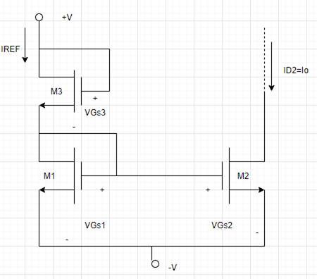
Consider the given circuit as shown below.
The transistor
From equation (1) put the value of
Also,
Now the load current is,
The load resistance will be,
Now the load current for
Now the change in load current,
Conclusion:
(c)
The load current
(c)
Answer to Problem 10.51P
Explanation of Solution
Given:
The circuit parameters are
The transistor parameters are
Calculation:
Consider the given circuit as shown below.
The transistor
From equation (1) put the value of
Also,
Now the load current is,
The load resistance will be,
Now the load current for
Now the change in load current,
Conclusion:
Want to see more full solutions like this?
Chapter 10 Solutions
MICROELECT. CIRCUIT ANALYSIS&DESIGN (LL)

- In the amplifier circuit in the figure, %3D R = 650kN, R, = 250kn, Rs = 5kn, R, = 4kn, Vpp = 18V, VSGQ = 3.0181V and transistor param eters are given as Vrp = -1.9V, k, = 40µA/V², W/L = 80 ve 1 = 0.02V-1 %3D A, la Find the sm all signal voltage gain of the amplifier circuit VDD R1 Cc2 RL R2arrow_forwardDesign a common emitter amplifier for a Vout of+-6.3V. Vcc is set to 9V. At x=1, Av=12.6 V/V and the dynamic range from 6.3V to -6.3V. Rout must be less than 100 ohms and Rin must be higher than 100 kohmsarrow_forwardThis problem is AC analysis problem. DC analysis is not needed to answer the question. A) If we assume that the peak voltage of Vbe must be less than 10 mV to avoid small signal violations determine the value of Rsig if Vi has a peak amplitude of 1 V and Is = 1mA. Hint: Don't forget r!! Answer: Rsig =. B) If you did the DC analysis on this problem and calculated Vc = 50 mV and Vs = -100 mV what is the maximum amplitude of the output voltage while the circuit stays in active mode. Answer: Vo,max =, When you "verify" a mode of operation you will need to calculate all three voltages (Vc, Ve, VE for BJTS and VG, Vs, Vp for MOSFETS) and show the correct two conditions are satisfied. Assume Capacitors acts like open circuits at DC and short circuits for AC. > Assume the following: 5V o Beta = 100 O VBE = 0.7 o V: (Thermal) = 26 mV o Vr (Threshold) = 2V O VA = - o For MOSFET saturation mode: assume: lp = K(VGs-Vr)? (Assume K = 10 mA/V²). 5kn C2 01 C1 Rsig 1kn 10k Vi IIs :C3 1mA -5Varrow_forward
- 3. In the figure shown below, Vmax is measured as 5.9 V and V min measured as 1.2V. 18] In the figure shown below, is measured as 5.9 V an (a) Determine the value of V.. (b) Determine the value of Vm. (c) Determine the modulation index. (d) Suppose we can change the value of V. What is the maximum value that we could use for Vm without causing overmodulation?arrow_forwardCoonsider the common emitter amplifier shown in figure below. Assume a β of 100, VBE = 0.7V, VT = 25mA and VA = 100V. Draw an equivalent DC model and determine the rπ, transconductance (gm) and ro. Draw an equaivalent AC model using the small-signal model Find an expression for vbe and vo in terms of the input voltagearrow_forward2. This is a small signal problem. Suppose the MOSFETS drawn have lp = 1 mA when VGS = 2.5 V, and Vth = 0.5 V. Suppose the BJTs drawn have Ic = 1 mA when VBE = 0.7 V. Av VDD = 5V VDD VDD T T Rc = 1 kn Vin RB2 = 10 kn RB1 = 10 kn w/li w Rp = 1 kn R₁ Vout (a) Derive voltage gain Ay and input impedance Zin assuming R₁ ➡8. (b) Plot Ay as a function of R, assuming R, is attached between Vout and ground. (c) Rederive Ay and Zin assuming Roo and after swapping the BJT and MOSFET. RLarrow_forward
- For the circuit given below Given Vsat=12V . I) Identify the stages II) Find the output voltagearrow_forwardQ1. For the MOSFET circuit below, input is sinusoidal signal of amplitude IV and frequency 50Hz. Find, the DC operating point, Plot the frequency response and Plot the input, output and transfer characteristics and find out the small signal equivalent. Assume an overdrive voltage of 0.2V Use MOSFET 500nm Library file provided. F Vdd=5V -=80 K R1 (1 1.20Farrow_forward35. The ac schematic of an NMOS common-source stage is shown in the figure below, where part of the biasing circuits has been omitted for simplicity. For the n- channel MOSFET M, the Transconductance 9m = 1mA/V, and body effect and channel length modulation effect are to be neglected. The lower cutoff frequency in Hz of the circuit is approximately at RD 10 ΚΩ M C 1μF R10 ΚΩarrow_forward
- what is the small signal model? ro of the transistors approach infinityarrow_forward35. The ac schematic of an NMOS common-source stage is shown in the figure below, where part of the biasing circuits has been omitted for simplicity. For the n- channel MOSFET M, the Transconductance 9m = 1mA/V, and body effect and channel length modulation effect are to be neglected. The lower cutoff frequency in Hz of the circuit is approximately at RD 10 ΚΩ V₁o M C 1uF R 10 ΚΩarrow_forwardDesign a common-emitter amplifier to provide a small-signal voltage gain of approximately -10. 1. Consider the circuit shown in Figure 1. Show the following calculations in your notebook: Calculate a value for Rc so that A, z –10 Calculate values for R1 and R2 so that the circuit is bias stable and near the center of the load line. (Note: Use the datasheet for the 2N5209 transistor to make your calculations more accurate). Vcc = 10 V R1 Rc Cc2 Cci RL Vs R, REj = 499 Q Figure 1: Common-emitter amplifier for part #1arrow_forward
 Introductory Circuit Analysis (13th Edition)Electrical EngineeringISBN:9780133923605Author:Robert L. BoylestadPublisher:PEARSON
 Delmar's Standard Textbook Of ElectricityElectrical EngineeringISBN:9781337900348Author:Stephen L. HermanPublisher:Cengage Learning
 Programmable Logic ControllersElectrical EngineeringISBN:9780073373843Author:Frank D. PetruzellaPublisher:McGraw-Hill Education
 Fundamentals of Electric CircuitsElectrical EngineeringISBN:9780078028229Author:Charles K Alexander, Matthew SadikuPublisher:McGraw-Hill Education
 Electric Circuits. (11th Edition)Electrical EngineeringISBN:9780134746968Author:James W. Nilsson, Susan RiedelPublisher:PEARSON
 Engineering ElectromagneticsElectrical EngineeringISBN:9780078028151Author:Hayt, William H. (william Hart), Jr, BUCK, John A.Publisher:Mcgraw-hill Education,