
Introductory Circuit Analysis (13th Edition)
13th Edition
ISBN: 9780133923605
Author: Robert L. Boylestad
Publisher: PEARSON
expand_more
expand_more
format_list_bulleted
Related questions
Question
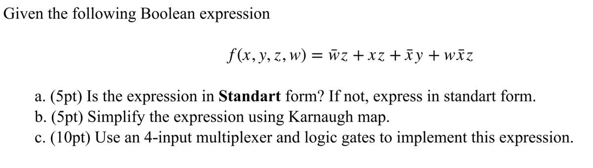

Transcribed Image Text:Given the following Boolean expression
f (x, y, z, w) = wz +xz +xy + wĀZ
a. (5pt) Is the expression in Standart form? If not, express in standart form.
b. (5pt) Simplify the expression using Karnaugh map.
c. (10pt) Use an 4-input multiplexer and logic gates to implement this expression.
Expert Solution
This question has been solved!
Explore an expertly crafted, step-by-step solution for a thorough understanding of key concepts.

Step by stepSolved in 2 steps with 2 images

Knowledge Booster


Learn more about
Need a deep-dive on the concept behind this application? Look no further. Learn more about this topic, electrical-engineering and related others by exploring similar questions and additional content below.Similar questions
- Write, and test using spim, an assembly language program that inputs apositive integer N from the user, followed by N integers. Your program should outputhow many of the N integers have a value greater than 496 but less than or equal to 8128.arrow_forwardIH.W: Draw a logic eircuit of the following Boolean expression before and after simplification using karnough map and Boolean expression. Y-AB+ AB A B Y 1 1arrow_forwardassembly languagearrow_forward
- Course: Digital Logic Design Please solve this question in a one hour. Solve it step by step clearly: Image is inside the image:arrow_forwardkarnaugh mapsarrow_forwardUsing D flip-flops, design a logic circuit for the finite-state machine described by the state assigned table in Figure P9.6. Present Next State Output State x=0 x=1 Y2V1 Y2Y1 Y2Y1 Z 00 00 01 01 10 88 00 11 00 00 10 0 11 00 10 1 I need a step by step solutionarrow_forward
- Logic Time diagramarrow_forward9.6 Using D flip-flops, design a logic circuit for the finite-state machine described by the state assigned table in Figure P9.6. Present Next State State Output x=0 x=1 Y2V1 Y₂Y Y2Y1 Z 00 00 01 0 01 00 11 0 10 00 10 0 11 00 10 1 Figure P9.6arrow_forwardDraw a logic diagram for part a and simplify the Boolean expression in part (a) using a karnaugh map for part b. The picture contains more details of the question.arrow_forward
arrow_back_ios
arrow_forward_ios
Recommended textbooks for you
- Introductory Circuit Analysis (13th Edition)Electrical EngineeringISBN:9780133923605Author:Robert L. BoylestadPublisher:PEARSON
 Delmar's Standard Textbook Of ElectricityElectrical EngineeringISBN:9781337900348Author:Stephen L. HermanPublisher:Cengage Learning
 Programmable Logic ControllersElectrical EngineeringISBN:9780073373843Author:Frank D. PetruzellaPublisher:McGraw-Hill Education
  Fundamentals of Electric CircuitsElectrical EngineeringISBN:9780078028229Author:Charles K Alexander, Matthew SadikuPublisher:McGraw-Hill Education
 Electric Circuits. (11th Edition)Electrical EngineeringISBN:9780134746968Author:James W. Nilsson, Susan RiedelPublisher:PEARSON
 Engineering ElectromagneticsElectrical EngineeringISBN:9780078028151Author:Hayt, William H. (william Hart), Jr, BUCK, John A.Publisher:Mcgraw-hill Education,
Introductory Circuit Analysis (13th Edition)
Electrical Engineering
ISBN:9780133923605
Author:Robert L. Boylestad
Publisher:PEARSON
Delmar's Standard Textbook Of Electricity
Electrical Engineering
ISBN:9781337900348
Author:Stephen L. Herman
Publisher:Cengage Learning
Programmable Logic Controllers
Electrical Engineering
ISBN:9780073373843
Author:Frank D. Petruzella
Publisher:McGraw-Hill Education
Fundamentals of Electric Circuits
Electrical Engineering
ISBN:9780078028229
Author:Charles K Alexander, Matthew Sadiku
Publisher:McGraw-Hill Education
Electric Circuits. (11th Edition)
Electrical Engineering
ISBN:9780134746968
Author:James W. Nilsson, Susan Riedel
Publisher:PEARSON
Engineering Electromagnetics
Electrical Engineering
ISBN:9780078028151
Author:Hayt, William H. (william Hart), Jr, BUCK, John A.
Publisher:Mcgraw-hill Education,