
The design parameters for the BJT differential amplifier with the active load and the mode voltage gain.
Answer to Problem D11.71P
The value of the differential voltage gain is
Explanation of Solution
Given:
The given circuit is shown in Figure 1
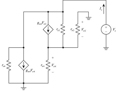
Figure 1
Calculation:
The expression for the input current is given by,
The expression to determine the value of the transconductance is given by,
The expression for the relation for the voltage for hybrid pie parameter.
Substitute
The value of the collector current
The value of the collector current
The expression to determine the expression for the diffusion resistance is given by,
Substitute
The value of the transconductance is calculated as,
Substitute
The expression to determine the value of the resistance
Substitute
The expression to determine the expression for the diffusion resistance is given by,
Substitute
The value of the transconductance is calculated as,
Substitute
The expression to determine the value of the resistance
Substitute
Substitute
The expression for the input current
Substitute
Substitute
The expression to determine the output resistance is given by,
Substitute
The value of the quiescent current is given by,
The small signal output resistance is calculated as,
The value of the output resistance is calculated as,
The required small signal circuit is shown in Figure 2
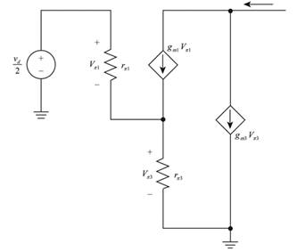
Figure 2
The expression for the transconductance is given by,
The expression for the differential voltage gain is given by,
The expression for the change in current is given by,
Consider the value of
Substitute the values in the above equation.
Substitute
Substitute
Substitute
Substitute
The value of gain is given by,
The expression for the input resistor is given by,
The value of expression for the differential input resistor is calculated as,
Conclusion:
Therefore, the value of the differential voltage gain is
Want to see more full solutions like this?
Chapter 11 Solutions
Microelectronics: Circuit Analysis and Design

- Design a common-source amplifier such that drain current is 11.33 Amp. State the tech parameters and assumptions made.arrow_forward11.13 The i-v characteristic of an n-channel enhancement MOSFET is shown in Figure P11.13(a); a standard amplifier circuit based on the n-channel MOSFET is shown in Figure P11.13(b). Determine the quiescent current ino and drain-to-source voltage vs 2.0 I= 25°C 1.8 1.6 Vas10 V- -9V- 1.4 1.2 8V- 1.0 0.8 7V- 0.6 0.4 5 V= 0.2 3 V- 1.0 2.0 3.0 4.0 5.0 6.0 7.0 8.0 9.0 10 Drain-source voltage vps. V (a) Rp VGD VDD VGS Va Drain current ip, Aarrow_forwardSketch DC and ac equivalent circuits and theoretically Analyze DC and ac analysis of a Single Stage JFET Common-Source Amplifier Circuit a. DC Equivalent Circuit b. ac Equivalent Circuit C. DC Analysis d. ac Analysisarrow_forward
- Calculate the collector current IC and the emitter collector voltage VCE of the amplifier shown in the figure and determine if it is in active region. shown in the figure and determine if it is in active region. Beta = 150.2. Calculate the input impedance Zi and output impedance Zo if ro = 7.5k.3. Calculate the voltage gain Av of the amplifier.arrow_forwardA. For the configuration shown below in 4(A), find the small signal voltage gain (Voutp-Voutm)/Vin B. For the configuration shown in 4(B), find the following parameters (a) DC value of output voltage, (b) input common mode range and (c) small signal voltage gain when all transistors are in saturation vou/Vin as indicated in the diagram; Assume no body bias on M1 ad M2 For this problem ONLY, assume the following device parameters V7, = \V| = 0.5V;K, = k ,' = 100 µA / V²,a, = a, = 0.01 VDD = 3V (10/1) M, M. (10/1) (10/1) M, |M, (10/1) Voutp 20kΩ м, (200/1) м, м, (10/1) м, Vin (1/1) м, M. (10/1) + Vin DC VAN M, 100HA (1/1) M, M, (10/1) (A) (B) V. =-1Varrow_forwarda) Calculate the VA voltage value.b) Given the input voltage (Vin) waveformin the above Op-amp circuit, Vtl (low)and Vtu (high) hysteresis crossoverCalculate the voltages. c) At the Vtl and Vtu transitions of the Vo voltageCalculate the position changes.arrow_forward
- determine transistor biasing (terminal voltages), current gain and voltage gainarrow_forwardQ1. (a) Consider the amplifier circuit in Figure Q1(a). Given the following: RI = 100 k2 R2 = 56 kN Rc =2 k2 Vcc = +8 V Assume the transistor has B = 100 and VBE(on) = 0.7 V. You may neglect Early effect and use VT = 26 mV. (i) Draw the DC equivalent circuit, then determine Iç and VCE. Draw the AC equivalent circuit using re model. Based on this, determine the parameters Av, Rin and Rout. (ii) Vcc Rc R1 R2 C3 Vout C2 Ci Vin Figure Q1(a)arrow_forwardWhat type of biasing circuit using in the common source JFET amplifier?arrow_forward
- A) Find and draw the equivalent re circuit model. Calculate the voltage gain.arrow_forwardQ For the following specifications Vez 10V lc 5 mA Is-20 MA A.--9 Design an Emitter stabilized (cmitter feedback) Bias circuit and ensure that the Q-point in the middle ofr the DC load linc.arrow_forwardThe DC Current Gain of a Transistor is Select one: a. Ratio of Collector Current to Base Current b. Ratio of Base Current to Collector Current c. Ratio of Emitter Current to Collector Current d. Ratio of Base Current to Emitter Currentarrow_forward
 Introductory Circuit Analysis (13th Edition)Electrical EngineeringISBN:9780133923605Author:Robert L. BoylestadPublisher:PEARSON
 Delmar's Standard Textbook Of ElectricityElectrical EngineeringISBN:9781337900348Author:Stephen L. HermanPublisher:Cengage Learning
 Programmable Logic ControllersElectrical EngineeringISBN:9780073373843Author:Frank D. PetruzellaPublisher:McGraw-Hill Education
 Fundamentals of Electric CircuitsElectrical EngineeringISBN:9780078028229Author:Charles K Alexander, Matthew SadikuPublisher:McGraw-Hill Education
 Electric Circuits. (11th Edition)Electrical EngineeringISBN:9780134746968Author:James W. Nilsson, Susan RiedelPublisher:PEARSON
 Engineering ElectromagneticsElectrical EngineeringISBN:9780078028151Author:Hayt, William H. (william Hart), Jr, BUCK, John A.Publisher:Mcgraw-hill Education,