
Videos
Consider the diff-amp in Figure P11.68. The PMOS parameters are:
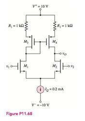
(a)
The open circuit differential mode voltage gain.
Answer to Problem 11.68P
The value of the differential mode voltage gain is
Explanation of Solution
Given:
The given circuit is shown in Figure 1
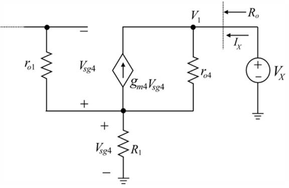
Figure 1
Calculation:
From above, the expression for the source to gate voltage is given by,
Apply KCL at node
Substitute
The expression for the transconductance of the second transistor is evaluated as,
Substitute
The internal output resistance of the second transistor is given by,
Substitute
The expression for the transconductance of the fourth transistor is evaluated as,
Substitute
The internal output resistance of the fourth transistor is given by,
Substitute
The expression to determine the value of the resistance
Substitute
The expression to determine the value of the open circuit differential mode voltage gain is given by,
Substitute
Conclusion:
Therefore, the value of the open circuit differential mode voltage gain is
(b)
To compare: The value of the open circuit differential mode voltage gain for the given changes with the value obtained in part (a).
Answer to Problem 11.68P
The value of the differential voltage gain is
Explanation of Solution
Given:
The given circuit is shown in Figure 1
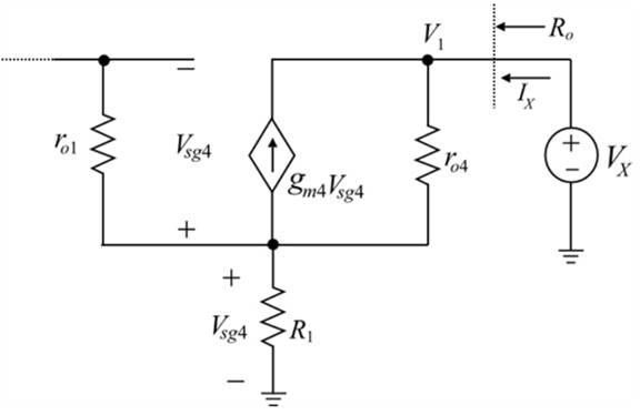
Figure 1
The value of resistance
Calculation:
When
The expression for the open circuit differential mode voltage gain is given by,
Substitute
When the resistance
Conclusion:
Therefore, the value of the differential voltage gain is
(c)
The value of the output resistance of the differential amplifier for part (a) and (b).
Answer to Problem 11.68P
The differential output resistance of the amplifier for part (a) is
Explanation of Solution
The given circuit is shown in Figure 1

Figure 1
Calculation:
The output resistance for the differential amplifier for the open circuit differential voltage gain is calculated as,
Substitute
The output resistance for the differential amplifier when
Substitute
Conclusion:
Therefore, the differential output resistance of the amplifier is
Want to see more full solutions like this?
Chapter 11 Solutions
Microelectronics: Circuit Analysis and Design


- Given a D-MOSFET circuit used as an amplifier with the following parameter: IDSS=12mA and a transconductance of gm=3.2 mS. Determine the DC drain to source voltage VDS and the AC output voltage if Vin=500 mV.arrow_forward"It is desirable for the following circuit, assuming the transistors are the same." A) Common fashion gain B) Differential gain mode C) Input resistance network D) CMRR E) What effect does the change in load resistance have on the circuit? Vcc Rc Re Qu, Vi PEE -VEEarrow_forwardQUESTION 6: Consider the circuit of Figure P11.3 with transistor parameters ß= 155 , V4=0, and VBE(on) = 0.66 V. The circuit is biased by V*= 6 V and V = -6 V. Design the circuit such that the Q-point values are Icı = Ic2 = 140 µA, and vo1 =vo2 = 1.2 V for vị = v2 = 0. Format : 98.34 Rc (kN) Format : 47.93 RE (kN) Ici RC RC v02 10a RE Figure P11.3arrow_forward
- A constant-current source is shown in Figure (Q1), the BJT information is: B = 100 • VA VBE = 0.7 V = 100 V If the collector voltage undergoes a change of 10 V while the BJT remains in the active mode, what is the corresponding change in the collector current? 5 V 4.3 Ка Figure (Q1)arrow_forward6. This problem involves designing a differential amplifier of the following figure. You may assume that the body and source terminal is shorted and you can neglect channel length modulation. Use the following MOSFET parameters: Parameter N-channel P-channel Units +1.10 -1.20 V 5. 2E-5 A/v 1.5E-5 a) Choose IBIAS for an output DC bias level Vo1(Dc) = Voz(DC)=3.00 V. b) Determine the voltage gain of the differential amplifier. c) Determine the magnitude of the small signal common mode gain. VDD = +5V RD1 5kQ RD2 5kO Voi0 o Vo2 M1 M2 W/L=80/2 w/L=80/2 ) IBIAS Vss = -5Varrow_forward10 In the circuit shown in Figure P11.10, a drain voltage of 0.1 V is established. Find the current ip for Vr = 1 V and k = 0.5 mA/V². 'p = 0.1 V D S VDD = 15 Varrow_forward
- 11.13 The i-v characteristic of an n-channel enhancement MOSFET is shown in Figure P11.13(a); a standard amplifier circuit based on the n-channel MOSFET is shown in Figure P11.13(b). Determine the quiescent current ino and drain-to-source voltage vs 2.0 I= 25°C 1.8 1.6 Vas10 V- -9V- 1.4 1.2 8V- 1.0 0.8 7V- 0.6 0.4 5 V= 0.2 3 V- 1.0 2.0 3.0 4.0 5.0 6.0 7.0 8.0 9.0 10 Drain-source voltage vps. V (a) Rp VGD VDD VGS Va Drain current ip, Aarrow_forwardA. Detemine the value of the collector resistor in an npn transistor amplifier with Bpc = 250, VBB = 2.5 V, Vcc = 9 V, VCE = 4 V, and Rg = 100 k2. B. Detemine Ic(sat) for the transistor in below Figure. What is the value of Is necessary to produce saturation? What minimum value of VIN is necessary for saturation? Assume VCE(sat) = 0 V. %3D +5 V 10 kN Rg VINO BDC = 150 1.0 MNarrow_forwardClass B Amplifier q1)If the input is 7.5Vp-p...DATA COLLECTION: What is the IL(peak)? a)7mA 6)mA 5)mA 4)mA q2) DATA COLLECTION: What is the Idc? a)3.84 b)4.82 c)3.82mA d)1.82mA q3)DATA COLLECTION: What is the input power in DC? Power input = 48.45mW Power input = 45.48mW Power input = 44.58mW Power input = 45.84mW q4) DATA COLLECTION: What is the output power in AC? a)18mW b)81mW c)11.8mW d)18.9mW q5)DATA COLLECTION: What is the power dissapated by each transistor? a)35.1mW b)53.1mW c)15.3mW d)13.5mW q6)DATA COLLECTION: What is the efficiency of class B amplifier? a)45% b)40% c)63% d)33% q7)arrow_forward
- 9 The NMOS transistor shown in Figure P11.9 has Vr = 1.5 V and K = 0.4 mA/V². If vg is a pulse with O to 5 V, find the voltage levels of the pulse signal at the drain output. 1 k2: VD VDD = 5 VE VG G VGarrow_forwardInstruction/s: Draw, Illustrate and label your schematic diagram before solving the problem.2.) Given a Collector -Feedback Biased transistor circuit with voltage at common collector is +10v ,base resistor is 100k ohms, Collector resistor is 10k ohms and Base current is 8.38 micro ampere, ,Voltage at Base-emitter junction is 0.7v. Determine Beta DC , Collector current and Voltage at collector-emitter junction. These might help as a guide to answer the problem...arrow_forwardTwo PNP transistors are connected to form a Darlington pair to create a single stage amplifier. Both transistors have the same B. Assume that is large such that 3+ 1 ~ B. Vcc 028² 028 9m2 RL 2+9m2 RL VIN PNP Darlington Pair Used as an Amplifier 1. If the Darlington pair is to be treated as a single transistor, what is the overall 3 if the "emitter current" is IOUT? OB² 9m2 Rp 1+9m2 RL RL 9m2 RL iOUT 2. Calculate the approximate expression for Ay. User1 and gm1 for the parameters of Q1 while 2 and for the parameters of Q2. Assume VA → ∞ for both transistors. 9m2 -9m2 RL 2 VOUTarrow_forward
 Introductory Circuit Analysis (13th Edition)Electrical EngineeringISBN:9780133923605Author:Robert L. BoylestadPublisher:PEARSON
 Delmar's Standard Textbook Of ElectricityElectrical EngineeringISBN:9781337900348Author:Stephen L. HermanPublisher:Cengage Learning
 Programmable Logic ControllersElectrical EngineeringISBN:9780073373843Author:Frank D. PetruzellaPublisher:McGraw-Hill Education
 Fundamentals of Electric CircuitsElectrical EngineeringISBN:9780078028229Author:Charles K Alexander, Matthew SadikuPublisher:McGraw-Hill Education
 Electric Circuits. (11th Edition)Electrical EngineeringISBN:9780134746968Author:James W. Nilsson, Susan RiedelPublisher:PEARSON
 Engineering ElectromagneticsElectrical EngineeringISBN:9780078028151Author:Hayt, William H. (william Hart), Jr, BUCK, John A.Publisher:Mcgraw-hill Education,