
Videos
a.
The value of
a.
Answer to Problem 11.43P
Explanation of Solution
Given:
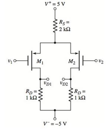
The given circuit is,

Calculation:
Consider the given figure,
Let equate the voltages,
Hence,
b.
The value of
b.
Answer to Problem 11.43P
Explanation of Solution
Given:
The given circuit is,

Calculation:
Consider the given figure,
Let equate the voltages,
Hence,
c.
The value of
c.
Answer to Problem 11.43P
Explanation of Solution
Given:
The given circuit is,
Calculation:
Consider the given figure,
Let equate the voltages,
Hence,
d.
The value of
d.
Answer to Problem 11.43P
Explanation of Solution
Given:
The given circuit is,
Calculation:
Consider the given figure,
Let equate the voltages,
Hence,
Want to see more full solutions like this?
Chapter 11 Solutions
Microelectronics: Circuit Analysis and Design


- A base biased transistor circuit with the following element values is given VBB = 10V, VCC = 10V, RB = 470kΩ +/- 5%, RC = 820Ω, β = 100. Find the max and min values of base current. Type your equations and results ..arrow_forwardThis problem is AC analysis problem. DC analysis is not needed to answer the question. A) If we assume that the peak voltage of Vbe must be less than 10 mV to avoid small signal violations determine the value of Rsig if Vi has a peak amplitude of 1 V and Is = 1mA. Hint: Don't forget r!! Answer: Rsig =. B) If you did the DC analysis on this problem and calculated Vc = 50 mV and Vs = -100 mV what is the maximum amplitude of the output voltage while the circuit stays in active mode. Answer: Vo,max =, When you "verify" a mode of operation you will need to calculate all three voltages (Vc, Ve, VE for BJTS and VG, Vs, Vp for MOSFETS) and show the correct two conditions are satisfied. Assume Capacitors acts like open circuits at DC and short circuits for AC. > Assume the following: 5V o Beta = 100 O VBE = 0.7 o V: (Thermal) = 26 mV o Vr (Threshold) = 2V O VA = - o For MOSFET saturation mode: assume: lp = K(VGs-Vr)? (Assume K = 10 mA/V²). 5kn C2 01 C1 Rsig 1kn 10k Vi IIs :C3 1mA -5Varrow_forwardA modulating signal f(t) has a maximum frequency of 18 kHz and peak value of 3volt, this signal is encoded using PCM. 1- Calculate the number of bits per sample if the number of levels is 130 2- Calculate the SNRQ if the average power of f(t) is 45 watt. 3- Calculate the minimum system bandwidth. e 7:20arrow_forward
- Determine Ic, Ig, lĘ respectively for the PNP transistor shown in the figure below. Assume Is = 5x10-15 A, B = 50, VT= 26mV, VA = ", and Rc = 0.1 KO. %3D 01 Vcc 2V 1.2 V- Rc Select one: Oa. 11.531 mA, 0.231 mA, 11.762 mA b. 5.766 mA, 0.115 mA, 5.881 mA O c 2.306 mA, 0.046 mA, 2.352 mA O d. None of thesearrow_forward19. For the circuit shown in Figure B19a, Va 20V Rc= 3k2 RB = 10k2 VCE Figure B19a Sketch the DC load line in the Graph B19. Calculate the Q point, if the zero signal base current is 50 µA and a =0.991. Mark the Q point in load line. Graph B19 arch (hp 立arrow_forward(b) Draw the ID - VD curves for this MOSFET for ±VD for V₁ = 0 and V₁ = 1 V. VȚ = 1V. n V₁ + p-type D ID V₁arrow_forward
- A (2-2-2) AOI is implemented with transistors allhaving W/L = 2/1. What are the worst-case valuesof τPLH and τPHL if VDD = 2.5 V and C =200 fF?arrow_forward/ Design a circuit using an n-channel E-MOSFET with the following datasheet specifications: Ixon) = 500 mA at VGS 10 V and VGS(h) = 1 V. Use a (+12 V) dc supply voltage with voltage divider bias. The voltage at the drain with respect to ground is to be (+7.78 V), the voltage at the source with respect to the ground is to be (+2.1 V), and the maximum current from the supply is to be 21.1 mA.arrow_forward2) Consider the circuit given below. (Assume: K-4mA/V', Vt=-1V, A=0, (K= µCox.(W/L)) da Perform DC analysis and calculate Va. Vsg, Vs, voltages, and Ip, gm, ro values bo Draw a small-signal equivalent circuit Co Calculate Av, Rin, Rout values as shown on the schematic Also ) satwaton mode Test for Fill inthe table VG VSG O2m A Rin Vs QUin ID vo Coo 9m Ro Av Rout Rin Routarrow_forward
- A MOSFET with k = 4.5 mA/V2 and VT = 3 V is used in the biasing circuit below. Determine the value of VGS. Options: (a) 0 V (b) 3 V (c) 6 V (d) 4.5 Varrow_forwardThe transistor parameters for the differential amplifier shown in Figure P11.32 are VT N = 0.5 V, k n = 80 µA/V2, W/L = 4, and λ = 0. (a) Find RD and IQ such that ID1 = ID2 = 80 µA and vO2 = 2 V when v1 = v2 = 0. (b) Draw the dc load line, and plot the Q-point for M2. (c) What is the maximum common-mode input voltage? Figure p11.32arrow_forwardFor the circuit of Figure 2. Carry out the analysis in DC and small signal with www.w www www.www Vt=0.7 V, Kn(W/L) = 4 mA/V. Ignore the Early effect. Determine: (a) The current in DC ID. (b) The gains vo/v₁, io/ii (c) The input resistance Rin and output resistance Rout. wwwwww 06402 www Ca HH {ama Ο ΜΩ www.11 Figura 2: 0.51 k www.li 12 V • 27 ΚΩ Ca +1₁ -0% 4.7 karrow_forward
 Introductory Circuit Analysis (13th Edition)Electrical EngineeringISBN:9780133923605Author:Robert L. BoylestadPublisher:PEARSON
 Delmar's Standard Textbook Of ElectricityElectrical EngineeringISBN:9781337900348Author:Stephen L. HermanPublisher:Cengage Learning
 Programmable Logic ControllersElectrical EngineeringISBN:9780073373843Author:Frank D. PetruzellaPublisher:McGraw-Hill Education
 Fundamentals of Electric CircuitsElectrical EngineeringISBN:9780078028229Author:Charles K Alexander, Matthew SadikuPublisher:McGraw-Hill Education
 Electric Circuits. (11th Edition)Electrical EngineeringISBN:9780134746968Author:James W. Nilsson, Susan RiedelPublisher:PEARSON
 Engineering ElectromagneticsElectrical EngineeringISBN:9780078028151Author:Hayt, William H. (william Hart), Jr, BUCK, John A.Publisher:Mcgraw-hill Education,