
Videos
Consider the differential amplifier shown in Figure 9.24(a). Assume thateach resistor is
(a)
The value of the worst case common mode gain.
Answer to Problem 9.62P
The value of the worst case common mode gain is
Explanation of Solution
Calculation:
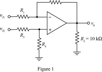
The given diagram is shown in Figure 1
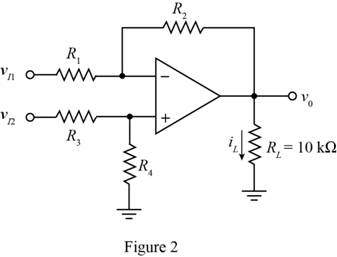
Mark the voltages and redraw the circuit.
The required diagram is shown in Figure 2
The expression for the common mode voltage gain is given by,
The expression for the value of the voltage
The expression for the voltage
Apply KCL at the inverting terminal.
Substitute
Substitute
The expression for the common node input voltage is given by,
The expression for the common node input voltage is given by,
Substitute
Substitute
In the above equation the worst case
For worst condition the value of the resistance
For worst condition the value of the resistance
For worst condition the value of the resistance
For worst condition the value of the resistance
Substitute
Conclusion:
Therefore, the value of the worst case common mode gain is
(b)
The value of the CMRR and the common mode gain.
Answer to Problem 9.62P
The value of
Explanation of Solution
Calculation:
The expression for the common mode gain is given by,
The expression for the differential voltage is given by,
Substitute
The expression for the voltage
The expression for the common mode voltage is given by,
Substitute
Substitute
Substitute
Substitute
Substitute
The expression for the
Substitute for
Substitute
Substitute
Substitute
Substitute
Substitute
Substitute
Conclusion:
Therefore, the value of
Want to see more full solutions like this?
Chapter 9 Solutions
MICROELECT. CIRCUIT ANALYSIS&DESIGN (LL)


- r:09 A moodle1.du.edu.om An application demands that sinusoidal pressure variation of 250 Hz be measured with no more than 2% dynamic error. In selecting a suitable pressure transducer from vendor catalog, you note that a desirable line of transducer has a fixed natural frequency of 500 Hz but that you have a choice of transducer damping ratio of between 0.5 and 1.5 in increments of 0.05. select a suitable transducer. The value of damping ratio is between the following values Select one: O a. 0.707 and 0.807 O b. 0.631 and 0.692 O c. 0.2356 and 0.5625 O d. 0.5215 and 0.5625 Previous page Next page 1 Aşsignmenarrow_forwardFor the circuit in the figure, extract the following as the formula according to r model and π model. a) IB, IC and IE currents b) The voltages at the X, B, C, E points and the voltage VCE c) Ri input resistance and output resistance Ro d) Av Voltage gains e) Low cutoff frequencies f) Formulate the high cutoff frequencies.arrow_forwardThe parameters in the circuit shown in Figure-4 are Vp 0.7 V, Vi=2.3 V, and Vzz = 5.6 V. Find and plot Vo versus Vi over the range of -10 Vi+10 V (Hint: You can consider input signal as sine wave of amplitude of +10 V and -10 V). Note: please solve within 30 minutes. Avoid plagiarism.arrow_forward
- Frequency Response of Multistage Amplifiers 27. In a certain two-stage amplifier, the first stage has critical frequencies of 230 Hz and 1.2 MHz. The second stage has critical frequencies of 195 Hz and 2 MHz. What are the dominant critical frequencies?arrow_forwardProblem 9.63 , except with R=1kOhm and a 100 Ohm load resistor from the op amp output pin to ground. Also find iofor each set of input conditions.arrow_forwardDefine and differentiate the following terms. Also Draw plots where required. You can use different symbols to denote each term a. Gain Cross over Frequency VS.Phase Cross over Frequency b. Phase Margin VS. Gain Margin c. Three Conditions of Stability in terms of phase cross-over frequency and gain-cross over frequency. Three Conditions of Stability in terms of phase margins and gain marginsarrow_forward
- QUESTION 5: Consider the ideal inverting summing amplifier in Figure 9.14(a). Design an ideal inverting summing amplifier to produce an output voltage of vo = -2.5(1.2v71 + 2v½ + 0.25v73) assuming the largest resistance in the circuit is 409 kO. R1 (kN) Format : 59.409378229784 R2 (kN) Format : 49.289 R3 (kN) Format : 706 Rf (kN) Format : 768.763 RF ww la R1 vy = 0 R2 R3 Figure 9.14(a)arrow_forwardQuestions: Draw output waveform for the following circuits if sinusoidal signal of 6V peak-to-peak with zero offset is applied at the input. Consider reference voltage VR = +2V R. VR Consider Zener voltage 2.5V Dz * R VR = -3V v,(f) 22arrow_forwardPlz solve both , i vll share positive feedback and vll upvote.... ASAP PLZZarrow_forward
- Determine the noise figure of an amplifier for which noise equivalent resistance Req = 25180 and Rt = 6000. It is driven by a generator whose output impedance is 500. It is given that constitutes a large enough mismatch.arrow_forwardI need to create a multistage amplifier. With the following specs.arrow_forwardDesign a three-stage amplifier that is impedance matched (use an emitter follower in stage 2) with an overall voltage gain of approximately 400. The phase of the input and output signal should be maintained. The amplifier should have a usable bandwidth of approximately 20MHz. As engineers you are expected to provide mathematical calculations, circuit diagrams and simulations in multisim software. The simulations should show a sample input signal, its output signal and frequency response plot of the three-stage amplifier.arrow_forward
 Introductory Circuit Analysis (13th Edition)Electrical EngineeringISBN:9780133923605Author:Robert L. BoylestadPublisher:PEARSON
 Delmar's Standard Textbook Of ElectricityElectrical EngineeringISBN:9781337900348Author:Stephen L. HermanPublisher:Cengage Learning
 Programmable Logic ControllersElectrical EngineeringISBN:9780073373843Author:Frank D. PetruzellaPublisher:McGraw-Hill Education
 Fundamentals of Electric CircuitsElectrical EngineeringISBN:9780078028229Author:Charles K Alexander, Matthew SadikuPublisher:McGraw-Hill Education
 Electric Circuits. (11th Edition)Electrical EngineeringISBN:9780134746968Author:James W. Nilsson, Susan RiedelPublisher:PEARSON
 Engineering ElectromagneticsElectrical EngineeringISBN:9780078028151Author:Hayt, William H. (william Hart), Jr, BUCK, John A.Publisher:Mcgraw-hill Education,