
Videos
Consider the class−AB output stage in Figure P8.48. The parameters are:
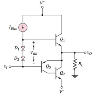
Figure P8.48
(a)
The value of
Answer to Problem 8.48P
Thevalue of the voltage
Explanation of Solution
Calculation:
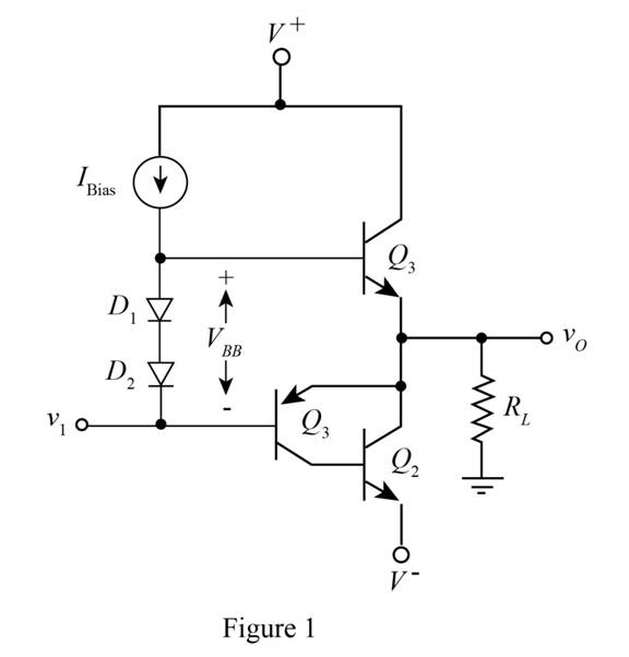
The given diagram is shown in Figure 1
The conversion from
The conversion from
The expression for the value of
Substitute
The expression for the value of the current
The expression for the value of the current
The expression for the value of the current
Substitute
The expression for the value of the current
The expression for the value of the current
The expression for the value of base to emitter voltage
The expression for the value of base to emitter voltage
The expression for the value of
Substitute
Substitute
Substitute
The expression for the value of base to emitter voltage
The expression for the value of base to emitter voltage
The expression for the value of the base to emitter voltage
Substitute
Substitute
Substitute
Substitute
The expression for the value of the current
Substitute
Substitute
Substitute
Substitute
The expression for the value of the voltage
Substitute
Conclusion:
Therefore, the value of the voltage
(b)
The value of
Answer to Problem 8.48P
The value of power delivered
Explanation of Solution
Calculation:
The expression for the value of the current
Substitute
The expression for the voltage
Substitute
The expression for the voltage
Substitute
The expression for the value of the voltage is given by,
Substitute
The expression for the value of the current for
Substitute
The expression for the value of the power delivered to the load is given by,
Substitute
The expression for the power delivered in the transistor of
Substitute
The expression for the power delivered in the transistor of
Substitute
The expression for the value of the current
Substitute
The expression for the value of the power dissipated in the transistor
Substitute
Conclusion:
Therefore, the value of power delivered
Want to see more full solutions like this?
Chapter 8 Solutions
MICROELECT. CIRCUIT ANALYSIS&DESIGN (LL)


- Sketch carefully the following signal.in dsp material or signal and systemarrow_forwardProblem #6: An abrupt p-n junction varactor is used to tune an oscillator shown in Figure 3. At zero bias voltage, the varactor has a junction capacitance of 4pF, Vbi 1.3V for GaAs. The active device has CD = 2pF and RD = 10W. The load bias has L₁ = 15nH and R₁ = 10W. What are the oscillation frequencies at (a) -20V (b) -10V and (c) OV? = L₁ R₁ C₁ (V) -RD FIGURE-3 www CDarrow_forwardSet up a midpoint bias for a JFET with IDSS = 14 mA and VGS(off) = -10 V. Use a 24 V dc source as the supply voltage. Show the circuit and resistor values. Indicate the value of ID. Indicate the value of VGS. Indicate the value of VDS.arrow_forward
- Plot the graphs of the outputs of the circuits in scale according to the input signal.and provide information about varactor structure and usage areasarrow_forward• Design a classical rectifier to deliver 100W into a resistive load from a 120V, 60HZ mains. ac Quantify the effect for different values of filter capacitance on: >average output voltage >output voltage ripple >Input current shape, harmonic content and THDarrow_forward........ (Figure-1) R. RB= 380kN,Rc= 1kN B = 100, VBB = Vcc=12V RB ww Vec CC ......... I, V CE СЕ V ВЕ BB Q-1-b) Describe briefly the input / output characteristics and application of Common Emitter BJT Configurationarrow_forward
- The positive peak value of output waveform for the given circuit diagram is.. (VPP of input is 18 V, Bias voltage is 3 V, Diode is germanium) R: D, VIN VouUT VaASarrow_forwardA 4.7 zener diode is connected to the base resistor. The left side of the resistor sits at about 12V. The right side of the biasing resistor is connected to the Zener and npn transistor. The Zener bias is 5mA. The base current needed is 80uA. What is the appropriate resistor for this circuit? (In kohms) Iarrow_forwardQuestiona. In an experiment the voltage required for the device is 9V dc but unfortunately the transformer available is of 220-6 Vdc. Design a circuit which can power the device (use only methods that we have studied excluding Zener diode)b. Explain the behavior of the following circuits if the input signal is triangular wave of peak voltage 5V and the biasing battery of 3Varrow_forward
- A certain npn silicon transistor has vBE=0.7 V for iB=0.1 mA at a temperature of 30°C. Sketch the input characteristic to scale at 30°C. What is the approximate value of vBE for iB = 0.1 mA at 180°C? (Use the rule of thumb that vBE is reduced in magnitude by 2 mV per degree increase in temperature.) Sketch the input characteristic to scale at 180°C.arrow_forwardc. For the circuit shown in Figure, determine lc and VCB. Assume the transistor to be made of Silicon. Ic RE=1.6 kn Rc=1.1 kn EE=8 V Vcc= 20 varrow_forward1-The output voltage of an emitter follower is a-In phase with Vin . b-Much greater than Vin. c-180° out of phase. d-Generally much less than Vin • 2-The ac emitter resistance of an emitter follower a-Equal the de emitter resistance. b-Is larger than the load resistance. c-Is B times smaller than the load resistance. d-Is usually less than the load resistance. 3-A common-base amplifier can be used when a-Matching low to high impedance. b-A voltage gain without a current gain is required. c-A high- frequency amplifier is needed. d-All of the above. 4-If the voltage generator is 5 mV in an emitter follower, the output voltage across the load is closest to a-5 mV. b-150mV. c-0.25 mV. d-0.5 mV.arrow_forward
 Introductory Circuit Analysis (13th Edition)Electrical EngineeringISBN:9780133923605Author:Robert L. BoylestadPublisher:PEARSON
 Delmar's Standard Textbook Of ElectricityElectrical EngineeringISBN:9781337900348Author:Stephen L. HermanPublisher:Cengage Learning
 Programmable Logic ControllersElectrical EngineeringISBN:9780073373843Author:Frank D. PetruzellaPublisher:McGraw-Hill Education
 Fundamentals of Electric CircuitsElectrical EngineeringISBN:9780078028229Author:Charles K Alexander, Matthew SadikuPublisher:McGraw-Hill Education
 Electric Circuits. (11th Edition)Electrical EngineeringISBN:9780134746968Author:James W. Nilsson, Susan RiedelPublisher:PEARSON
 Engineering ElectromagneticsElectrical EngineeringISBN:9780078028151Author:Hayt, William H. (william Hart), Jr, BUCK, John A.Publisher:Mcgraw-hill Education,