
Videos
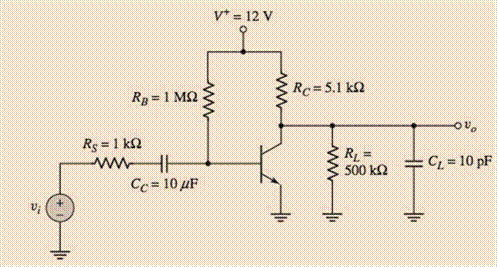
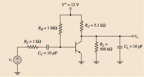
The parameters of the transistor in the circuit in Figure P7.40 are
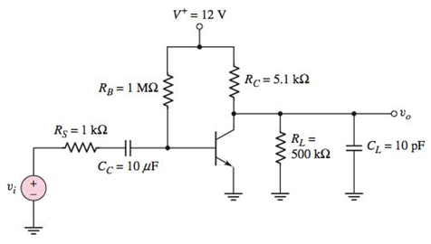 Figure P7.40
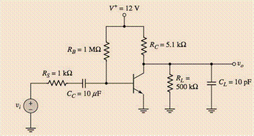
a.
To draw: Three equivalent circuits that represent the amplifier in the low frequency range, mid-band range and the high frequency range.
Answer to Problem 7.40P
Three equivalent circuits that represent the amplifier in the low frequency range, mid-band range and the high frequency range are shown in Figure 1, 2 and 3 respectively.
Explanation of Solution
Given:
The diagram is given as:
Calculation:
Calculate the value of current
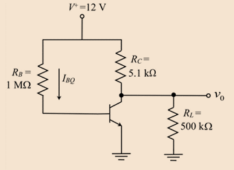
Applying Kirchhoff s voltage law in the above loop:
Here,
Substituting
The quiescent collector current
Here,
Substituting
Evaluating the resistance
Here,
Evaluating the transconductance
Substituting
Figure 2 shows the low −frequency small signal transistor with the output resistance
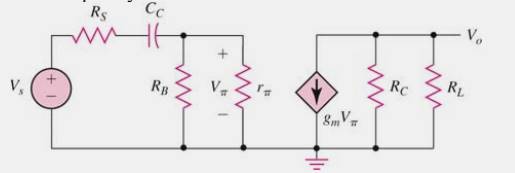
Figure 1
In the mid-frequency range, the coupling and bypass capacitors are short-circuited and the load capacitors are open-circuited.
It shows the mid-frequency small signal transistor with the output resistance
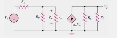
Figure 2
In the high-frequency range, the coupling and bypass capacitors are short-circuited and the load capacitors are included.
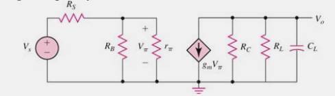
Figure 3
Hence, the three equivalent circuits that represent the amplifier in the low-frequency range, mid-band range, and high-frequency range are plotted.
b.
To sketch: The bode magnitude plot.
Answer to Problem 7.40P
The sketch of bode magnitude plot is shown in Figure 4.
Explanation of Solution
Given:
The diagram is given as:
Calculation:
Consider the values, calculated in part (a).
The effect of the coupling capacitor
The figure shows the bode plot for the circuit having a combination of a coupling capacitor and load capacitor:
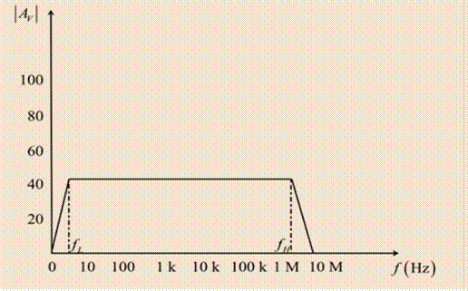
Figure 4
Hence, the bode magnitude plot is sketched.
c.
The values of the
Answer to Problem 7.40P
The values are:
Explanation of Solution
Given:
The diagram is given as:
Calculation:
Evaluating the midband gain by short-circuiting the coupling and bypass capacitors and open-circuiting the load capacitors.
Substituting the values,
Evaluating the gain in dB:
Substituting
Hence, the value of gain
Evaluating the equivalent resistance
Substituting
Evaluating the time constant
Substituting
Evaluating the equivalent resistance
Substituting
Evaluating the time constant
Substituting
Evaluate the lower corner frequency
Substituting
Evaluated the upper corner frequency:
Substitute
Want to see more full solutions like this?
Chapter 7 Solutions
MICROELECT. CIRCUIT ANALYSIS&DESIGN (LL)
Additional Engineering Textbook Solutions
Electronics Fundamentals: Circuits, Devices & Applications
ANALYSIS+DESIGN OF LINEAR CIRCUITS(LL)
Fundamentals of Applied Electromagnetics (7th Edition)
Engineering Electromagnetics
Loose Leaf for Engineering Circuit Analysis Format: Loose-leaf
Programmable Logic Controllers


- In the self-bias circuit of Figure 7.80 a. Draw the transfer characteristic curve of the device. b. Draw additional circuit equations on the same graph. Find c.lDQ and VGSQ. d. Calculate VDS , VD, VG, Vs. ...arrow_forward12- A DVM measure... a- peak value. b- RMS value. Average value. d- peak to peak value. 13 The study of energy distribution across the frequency spectrum of a given electrical signal is done by a Distortion meter b-wave analyzer.arrow_forwardEXERCISE PROBLEM *Ex 7.13: The transistor in the circuit in Figure 7.60 has parameters B= 125, VBE(on) = 0.7 V, VA = 200 V, C = 24 pF, and C= 3 pF. (a) Calculate the Miller capacitance. (b) Determine the upper 3 dB frequency. (c) Determine the small-signal midband voltage gain. (Ans. (a) CM = 155 pF, (b) fH = 1.21 MHz, (c) A] = 37.3)arrow_forward
- The message signal m(t) into a FM modulator with the parameter kf=25 is shown in the following figure.a) Express the FM signal in time domain.b) Calculate and plot the frequency deviation in Hz.c) Calculate and plot the phase deviation in radians.arrow_forwardA) A Varactor tuned oscillator (VTO) circuit is generating 3.56MHZ, with a Varactor capacitance 20 pF and tuning voltage 7.5 V. Calculate the following: 22 1) The inductor value of VTO circuit. 2) Oscillating frequency of VTO at the Varactor maximum capacitance. ks)arrow_forwardQuestion 2 (a) Briefly explain the advantage of the following Amplitude Modulation (AM) type and state ONE (1) application for each AM type: i. Double Sideband Full Carrier (DSBFC) ii. Double Sideband Suppressed Carrier (DSBSC) iii. Single Sideband (SSB). (b) The AM waveform for the modulated signal is illustrated in Figure 1. i. Calculate the percentage of modulation index, m. ii. State the type of the modulated signal. Justify the answer. iii. Write the equation for the modulated signal. iv. Calculate the percentage of power efficiency. 3V -1IV Figure 1arrow_forward
- Derive the transfer function of the electric circuits.arrow_forwardQ2. For the scheme shown in Figure Q2, i. Draw the spectrum of the baseband signal (multiplexer output) for the multiplexer. ii. Determine the bandwidth of the baseband signal (multiplexer output) for the multiplexer. i. Determine the minimum transmission bandwidth of the multiplexer. Explain, briefly, the modification needed for the multiplexer in the figure to achieve this bandwidth. 4 kHz cos 10,000xt Basebund signal cos 24,000mt cos 2000mt cos 32,000nt Figure Q2arrow_forwardOne input to a conventional AM modulator is a 600 kHz carrier with amplitude of 22 V. The second input is a 20 kHz modulating signal that is of sufficient amplitude to cause a change in the output wave of +9 V. Determine: a. Upper and lower side frequencies. b. Percent modulation. c. Peak amplitude of the modulated carrier and the upper and lower side frequency voltages. d. Maximum and minimum amplitudes of the envelope. e. Expression for the modulated wave. Then, f. Draw the output spectrum. g. Sketch the output envelope.arrow_forward
- After getting the formula of FM and PM moducation signal, how can I sketch this one.arrow_forwarddrive a formula for (SNR) of sinusoidal signal has been sampled and quantized.arrow_forward(a) Design the circuit shown in Figure P7.18 such that Ipo = 0.8 mA, VDsQ = 3.2 V, Rin K, = 0.5 mA/V², VTN = 1.2 V, and A = 0. (b) What is the midband volt- age gain? (c) Determine the magnitude of the voltage gain at (i) f = 5 Hz, (ii) f = 14 Hz, and (iii) f = 25 Hz. (d) Sketch the Bode plot of the voltage gain magnitude and phase. 160 k2, and fr 16 Hz. The transistor parameters are ass VDD =9 V Rp R1 Rin 1 O vO Cc Rs = 0.5 k2 R2 Figure P7.18 ww wwarrow_forward
 Introductory Circuit Analysis (13th Edition)Electrical EngineeringISBN:9780133923605Author:Robert L. BoylestadPublisher:PEARSON
 Delmar's Standard Textbook Of ElectricityElectrical EngineeringISBN:9781337900348Author:Stephen L. HermanPublisher:Cengage Learning
 Programmable Logic ControllersElectrical EngineeringISBN:9780073373843Author:Frank D. PetruzellaPublisher:McGraw-Hill Education
 Fundamentals of Electric CircuitsElectrical EngineeringISBN:9780078028229Author:Charles K Alexander, Matthew SadikuPublisher:McGraw-Hill Education
 Electric Circuits. (11th Edition)Electrical EngineeringISBN:9780134746968Author:James W. Nilsson, Susan RiedelPublisher:PEARSON
 Engineering ElectromagneticsElectrical EngineeringISBN:9780078028151Author:Hayt, William H. (william Hart), Jr, BUCK, John A.Publisher:Mcgraw-hill Education,