
Videos
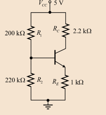
For the circuit in Figure 7.41(a), the parameters are,
(i)
a.
The midband current gain.
Answer to Problem 7.10EP
The value of mid-band current gain
Explanation of Solution
Given:
The parameters for the given circuit:
Drawing the DC equivalent circuit for the given circuit:
Evaluating the Thevenin equivalent voltage at the base terminal:
Evaluating the Thevenin equivalent resistance at the base terminal:
Drawing the DC equivalent circuit as shown below:
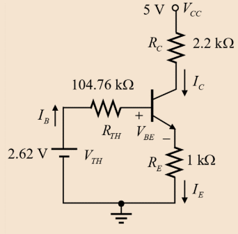
Evaluating the value of base current
Evaluating the value of collector current
Evaluating the value of small signal parameters
Evaluating the value of small signal parameters
Drawing the small-signal equivalent circuit for the mid band current gain:
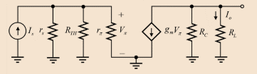
Applying the nodal analysis at the node
Applying the current division rule at the output node:
Evaluating the value of mid band current gain
Hence, the value of mid-band current gain
b.
The Miller capacitance CM for the given values of the
Answer to Problem 7.10EP
The Miller capacitances for the both cases are:
Explanation of Solution
Given:
The parameters for the given circuit:
The value of the capacitances are given as:
( i ) The value of capacitance
Evaluating the value of Miller capacitance for
Hence, the value of Miller capacitance for
(ii)
The value of capacitance:
Evaluating the value of Miller capacitance for
Hence, the value of the Miller capacitance for
c.
The upper 3-dB frequency for the given values of the
Answer to Problem 7.10EP
The 3-dB frequencies for the both cases are:
Explanation of Solution
Given:
The parameters for the given circuit:
The value of the capacitances are given as:
(i)
The value of Miller capacitance for
Since,
Evaluating the upper
Hence, the upper
(ii)
The value of Miller capacitance for
Since,
Evaluating the upper
Hence, the upper
Want to see more full solutions like this?
Chapter 7 Solutions
MICROELECT. CIRCUIT ANALYSIS&DESIGN (LL)


- Design a CE voltage-divider configuration with the indicated ac parameters. That is, determine the required values of R1, R2, Rc, and RE. Also, determine the expected output voltage if the input voltage is equal to 0.001 Vrmsarrow_forwardFrom the figure shown, when S1 is at 1 : up position; the following statement is not correct except: (a) Collector-emitter voltage of Q1 is approximately zero (b) the LED will illuminate (c) the base voltage of Q2 is equal to 9 V (d) (b) and (c)arrow_forwardA stabilization circuit has a stability factor of 0.04 and an internal resistance of 5 2. The unstabilized voltage can vary between 75 and 100 V, and the load current can vary from 40 to 80 mA. Determine the maximum and minimum values for the stabilized load voltage.arrow_forward
- The controlling parameter in MOSFET is a) Vds b) lg c) Vgs d) Isarrow_forwardFrom the figure shown, when S1 is at 1 (toggle at up position) the following statement is not correct except (a) the LED will illuminate b) a and c (c) the base voltage of Q2 is equal to 9 V (b) Collector-emitter voltage of Q1 is approximately zeroarrow_forwardN-channel Mosfet compared to P channel mosfetWhich of the following is true?A) It is faster.B) It has a lower input impedance.C) It has a lower noise level.D) nonearrow_forward
- we can see the following signal at which point of the modulator? 6 A Modulating signal D Carrier AM output В B D None of these C Cor D A This signal will never be presented in this modulatorarrow_forwardSmall amount of space it takes on a chip O All of the above 7. The main types of field effect transistor are O BJT and FET O UJT and FET O JFET and MOSFET O None of the above 9.The arrow on the symbol of MOSFET indicat that it is a N-channel MOSFET the direction of electrons O the direction of conventional current flow O that it is a P-channel MOSFETarrow_forwardIn a MOSFET amplifier, the AC input signal is applied at gate terminal and the amplified output is taken at source terminal. common emitter common gate common source common drainarrow_forward
- The transistor has the following properties: hre hrE B= 100, IVBel = 0,6v, V7 = 26mV and VA = , The resistor values are Ras#44k0, Re 22kn, Re#3.9kn, Rc#1.5ka. Collector current is 1.5mA. Calculate AC voltage gain V./Vi. Vcc Ru RE Vm-0.6V B100 Ca HH Vo Rn2 Rc Answer:arrow_forwardfor the given circuit, Vcc=50v, VBB=2v , Rc%3D30 k0, RB=50KO, VCE=0.134v and ?B=100. what is the type of the transistor ? what is transistor statues Rc Rg Vcc VE VBBarrow_forwardWhen an n-channel D-MOSFET has Ip > Ipss, it Is operating in the enhancement mode Is forward biased Is operating in the depletion mode Will be destroyedarrow_forward
 Introductory Circuit Analysis (13th Edition)Electrical EngineeringISBN:9780133923605Author:Robert L. BoylestadPublisher:PEARSON
 Delmar's Standard Textbook Of ElectricityElectrical EngineeringISBN:9781337900348Author:Stephen L. HermanPublisher:Cengage Learning
 Programmable Logic ControllersElectrical EngineeringISBN:9780073373843Author:Frank D. PetruzellaPublisher:McGraw-Hill Education
 Fundamentals of Electric CircuitsElectrical EngineeringISBN:9780078028229Author:Charles K Alexander, Matthew SadikuPublisher:McGraw-Hill Education
 Electric Circuits. (11th Edition)Electrical EngineeringISBN:9780134746968Author:James W. Nilsson, Susan RiedelPublisher:PEARSON
 Engineering ElectromagneticsElectrical EngineeringISBN:9780078028151Author:Hayt, William H. (william Hart), Jr, BUCK, John A.Publisher:Mcgraw-hill Education,