
Videos
Let
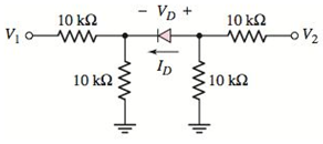
Figure P2.57
(a).
The values of
Answer to Problem 2.57P
Explanation of Solution
Given Information:
The given circuit is shown below.

Calculation:
Assuming the diode is in cutoff mode.
Applying voltage division rule:
The voltage across diode:
Hence, the diode is biased in reverse region. The assumption is correct and the value of diode current will be zero.
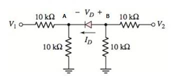
(b).
The values of
Answer to Problem 2.57P
Explanation of Solution
Given Information:
The given circuit is shown below.
Calculation:
Assuming the diode is in cutoff region.
Applying voltage division rule:
The voltage across diode:
Hence, the diode is biased in forward region. The assumption is incorrect.
Replacing the diode with its cut-in voltage:
The modified figure is:
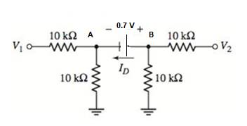
The node AB is a super node. Applying Kirchhoff’s current law at super node:
Adding equation 1 and 2:
From equation (1):
Applying Kirchhoff’s current law at node B:
(c).
The values of
Answer to Problem 2.57P
Explanation of Solution
Given Information:
The given circuit is shown below.

Calculation:
Assuming the diode is in cutoff mode.
Applying voltage division rule:
The voltage across diode:
Hence, the diode is biased in reverse region. The assumption is correct and the value of diode current will be zero.
(d).
The values of
Answer to Problem 2.57P
Explanation of Solution
Given Information:
The given circuit is shown below.

Calculation:
Assuming the diode is in cutoff region.
Applying voltage division rule:
The voltage across diode:
Hence, the diode is biased in forward region. The assumption is incorrect.
Replacing the diode with its cut-in voltage:
The modified figure is:

The node AB is a super node. Applying Kirchhoff’s current law at super node:
Adding equation 1 and 2:
From equation (1):
Applying Kirchhoff’s current law at node B:
Want to see more full solutions like this?
Chapter 2 Solutions
MICROELECT. CIRCUIT ANALYSIS&DESIGN (LL)


- Q4 (a) Find the current through the diode, In in the circuit shown in Figure B.1 if the SUTM A UTM BUTM UT UTM SUTM UTM UTM UT 10 V 50 A SUM B UT UTM BUTM SUTM SUTM UTM SUTM UTMU UTM UT M BUTM S UTM UTM UTM UT M BUT UTM UTM UTM UT UTM S UTM UTarrow_forwardA diode circuit is given in the below figure, in which two diodes are connected in series and their saturation currents are Is1 =10-¹6 A and Is2 =10-¹4 A. If the applied source voltage is 1 V, calculate the currents IDI and ID2 and the voltage across each diode VDI and VD2. IDI Ī Vpl + D₂ VD2arrow_forwardFor circuit given in Figure 3 use Complete Diode Modeland find the voltage across R1 and R2 and total current flowing in this circuit. Given that diode forward resistance is 15 Ohms for D1 and 10 Ohms for D2, also reverse current flowing acrossD2 is 20 micro Amperes. DI Ri 50 2 D2 Rz100 N www 10 V R3150 2 wwwarrow_forward
- Given the following circuit with VDD= 9.2 V, R=2.3 k2, then the current Iis: Use the CVD model for the diode, with VD = 0.65 V. I VDD a. 0.004000 A O b. 3.717391 A OC. 0 A d. 4.000000 A e. 0.003717 A R + VD -arrow_forwardQ2:- Find the level of V, for each circuit shown in the Figure below. Also, determine the status of each diode; if it is forward or reverses biasing. Assume all diodes are silicone with 0.7v drop. +5 V +15 V -10 V ER DI +5 Vo4 +5 Vo4 -5 Vo -5VoKD2 +5Vo D2 +5 VOK3 D3 -10 Vo D4 -5 Vo4 (a) (b) (c) +어arrow_forwardFigure Q2(a) shows the characteristic curve of a Zener diode. Analyse the characteristic curve to identify the approximate minimum Zener current Izk(min) and the approximate Zener voltage, Vz at IZK. -10 -9 -8 -7 -6 -5 -2 -1 Vz (V) + 1 3 4 6 7 8 Iz (mA) Figure Q2(a) Analyse the circuit in Figure Q2(b) to identify the minimum input voltage required to keep the diode in Zener region based on the values of the minimum Zener current and the approximated Zener voltage found in Question 2(a). R 1k2 VIN Figure Q2(b)arrow_forward
- A diode used in the Figure Q2 (a), has a characteristic as shown by the I-V (a) graph. Obtain the operating point for the diode in the given circuit and sketch the load- line for the circuit. In [mA] 100 Si 80 252 60 2.5V 40 20 + VD [V] 2.5 0.5 1 1.5 Figure Q2 (a) Wrarrow_forward4kN 2V Determine the state of diode for the circuit shown. find ID and VD. Assume simplified model for the diode. (Diode is Silicon). 4k2 2V 1k2. 0.7V O -0.375 mA, 0.4 V, off O -0.67 mA, -0.24 V, on O -1.5 mA, 0.7 v, off O 2.04 mA, -8 V, onarrow_forwardIn the following figure V, = 0 V and V2 = 8 V , which diode will conduct( assume ideal diodes) D, IkO ww V • D; IkQ 10k2 V, - ww E. D,only F. Dzonly G. D, and D2 H. neither D, nor D2 Dzonly neither D, nor D2 D1 and D2 D1onlyarrow_forward
- ii) Analyse the circuit shown in below Figure. 2, assume diodes as silicon diode. Calculate: a. Vout b. IR3 c. Ip2 VCC 16V D1 D4 V3 10 V R1 2.2kQ D5 D2 Vout R3 2.8kQ IR3 Ip2 R2 4.7 kQ D3 V1 2.2 V V2 15Varrow_forwardGiven the following circuit with VDD = 9.5 V, R = 3.2 k2, then the current Iis: Use the CVD model for the diode, with VD = 0.65 V. VDD I a. 0 A O b. 0.002766 A c. 0.002969 A d. 2.968750 A e. 2.765625 A R N V₂arrow_forwardV₂ VD,on = 800mV for the constant-voltage diode model. (1) Plot the input/output characteristics of the circuits below (a-c) using a constant-voltage diode model. Also, assume that VB = 1V. Vin D₁ VB +1 + R₁ Vout (a) Vin D₁ + R₁ (b) VB + Vout Vin VB R₁ D₁ (c) MMK + Voutarrow_forward
 Introductory Circuit Analysis (13th Edition)Electrical EngineeringISBN:9780133923605Author:Robert L. BoylestadPublisher:PEARSON
 Delmar's Standard Textbook Of ElectricityElectrical EngineeringISBN:9781337900348Author:Stephen L. HermanPublisher:Cengage Learning
 Programmable Logic ControllersElectrical EngineeringISBN:9780073373843Author:Frank D. PetruzellaPublisher:McGraw-Hill Education
 Fundamentals of Electric CircuitsElectrical EngineeringISBN:9780078028229Author:Charles K Alexander, Matthew SadikuPublisher:McGraw-Hill Education
 Electric Circuits. (11th Edition)Electrical EngineeringISBN:9780134746968Author:James W. Nilsson, Susan RiedelPublisher:PEARSON
 Engineering ElectromagneticsElectrical EngineeringISBN:9780078028151Author:Hayt, William H. (william Hart), Jr, BUCK, John A.Publisher:Mcgraw-hill Education,