
Concept explainers
The currents
Answer to Problem 13.1EP
The currents are:
Explanation of Solution
Given:
The bias circuit and input stage portion of 741 op-amp circuit is shown below.
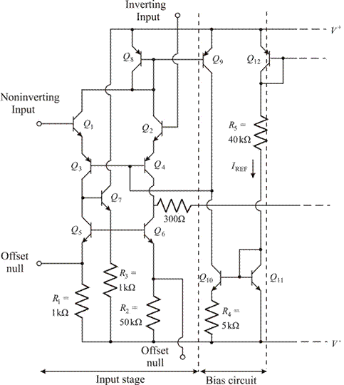
Figure 1
Resistance
Bias voltages are:
The base current is considered to be 0 A.
The base emitter voltages are:
Calculation:
Consider the given circuit. The formula for reference current that is established in the circuit branch consists of transistors
Transistors
Where,
Substitute the given values in the above equation.
By trial and error method,
For the given circuit, if the base current is neglected, then the collector current through transistors
Substituting the values,
Want to see more full solutions like this?
Chapter 13 Solutions
MICROELECT. CIRCUIT ANALYSIS&DESIGN (LL)


- (P. 6) For a particular junction for which C₁0 = 0.6 pF, Vo = 0.75 V, and m= 1/3, find C, at reverse-bias voltages of 1 V and 10 V.arrow_forward4) Consider the clamping circuit below, assume Vref=3 V and Vin=5sin(wt) ..Draw the output voltage waveform. Clearly mark the max and min of the voltage.. Vrefarrow_forwardThe Pinch off voltage for N- Channel JFET is -3V, maximum saturated drain current 8mA and the value of VGS is -1.5 V. Calculate drain current, a. 18 mA b. 2 mA c. 2.5 mA d. 4 mAarrow_forward
- Q. Choose the correct answer from the following: 2. A three-phase half-wave controlled converter is constructed using 3 SCR devices. The circuit is supplying an R load with a< 30°. As such, each SCR device would conduct for a) 60° each cycle b) 120° each cycle c) 180° each cycle d) 360° each cycle 4. A thyristor has a maximum allowable junction temperature of 120°C and the ambient temperature is 40°C. If thermal resistance is 1.6° C/W, the maximum allowable internal power dissipation is: a. 20 W b. 50 W c. 92 W d. 128 W 6. In reverse blocking state of a thyristor: a) junction J2 is in reverse bias and J1, J3 is in forward bias. b) junction J3 is in forward bias and J1, J2 in reverse bias. c) junction J1, J3 is in reverse bias and J2 is in forward bias. d) junction J1 and J2 is in forward bias and J3 is in reverse bias.arrow_forwardBA certain op-amp has an open-loop gain of 80,000. The maximum saturated output levels of this particular device are + 12 when the de supply voltages are ±15. If a differential voltage of 0.15 mV rms is applied between the inputs, what is the peak-to-peak value of the output?arrow_forwardIn series compensation, if the series applied voltage is in quadrature with the liner current: A. The series compensation cannot supply or absorb reactive power B. The series compensation can only supply active power C. The series compensation can only absorb active power D. The series compensation cannot supply or absorb active powerarrow_forward
- The Pinch off voltage for N-Channel JFET is -3V, maximum saturated drain current 8mA and the value of VGS is -1.5 V. Calculate drain current, a. 4 mA b. 2.5 mA c. 2 mA d. 18 mAarrow_forwardThermistor giving output of 0.5 mv for each degree change in temperature. Find the word length required when its output passes through Analog to digital converter if temperature from 0 to 200 degree Celsius are to be measured with a resolution of 0.5 degree Celsius.arrow_forwardSketch the de load line, quiescent collector current, quiescent voltsge, input power, output power and maximum efficiency of the circuit shown an Figure. The input results in a base current of 5 mA peak to peak What maximum output power can be delivered by the circuit, if the input voltage is changed resulting in a base current of 10mA peak to peak and hence find the maximum etficiency. cc=15 V R =18 2 -25arrow_forward
- The Pinch off voltage for N-Channel JFET is -3V, maximum saturated drain current 8mA and the value of VGS is -1.5 V. Calculate drain current.arrow_forwardThe arrow on the symbol of MOSFET indicates O a. that it is a N-channel MOSFET O b. the direction of conventional current flow O c. that it is a P-channel MOSFET O d. the direction of electronsarrow_forwardHow can I add two voltages values together with on op amp? Using op amps, how to make an AD Converter? A DA Converter? What components determine the frequency of an astable, 555 oscillator? Draw the circuit. Draw a circuit for both an astable and a monostable, 555 multivibrator. What is the duty cycle and percentage duty cycle of a pulse train or square wave? What is the overshoot, rise time, fall time, and pulse width of a pulse and where on the waveform is each measured?arrow_forward
 Introductory Circuit Analysis (13th Edition)Electrical EngineeringISBN:9780133923605Author:Robert L. BoylestadPublisher:PEARSON
 Delmar's Standard Textbook Of ElectricityElectrical EngineeringISBN:9781337900348Author:Stephen L. HermanPublisher:Cengage Learning
 Programmable Logic ControllersElectrical EngineeringISBN:9780073373843Author:Frank D. PetruzellaPublisher:McGraw-Hill Education
 Fundamentals of Electric CircuitsElectrical EngineeringISBN:9780078028229Author:Charles K Alexander, Matthew SadikuPublisher:McGraw-Hill Education
 Electric Circuits. (11th Edition)Electrical EngineeringISBN:9780134746968Author:James W. Nilsson, Susan RiedelPublisher:PEARSON
 Engineering ElectromagneticsElectrical EngineeringISBN:9780078028151Author:Hayt, William H. (william Hart), Jr, BUCK, John A.Publisher:Mcgraw-hill Education,