
Videos
(a)
The small signal parameters for each of the transistor and the value of the composite transconductance for the given specifications.
(a)
Answer to Problem 11.80P
The value of the small signal parameters are
Explanation of Solution
Given:
The given diagram is shown in Figure 1
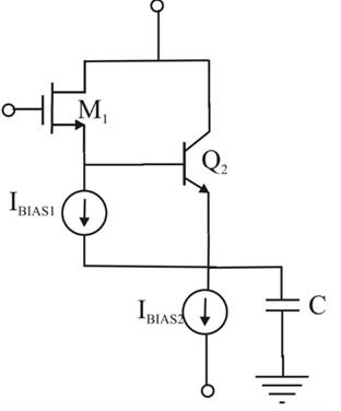
Figure 1
Calculation:
The expression to determine the value of the emitter current of the second transistor is calculated as,
The expression to determine the value of the current
Substitute
The value of the transconductance
The expression to determine the value of the small signal resistance is given by,
Substitute
The value of the drain current
The value of the transconductance
Substitute
The expression to determine the value of the composite transconductance is given by,
Substitute
Conclusion:
Therefore, the value of the small signal parameters are
(b)
The small signal parameters for each of the transistor and the value of the composite transconductance for the given specifications.
(b)
Answer to Problem 11.80P
The value of the small signal parameters are
Explanation of Solution
Given:
The given diagram is shown in Figure 1

Figure 1
Calculation:
The expression to determine the value of the emitter current of the second transistor is calculated as,
The expression to determine the value of the current
Substitute
The value of the transconductance
The expression to determine the value of the small signal resistance is given by,
Substitute
The value of the drain current
The value of the transconductance
Substitute
The expression to determine the value of the composite transconductance is given by,
Substitute
Conclusion:
Therefore, the value of the small signal parameters are
Want to see more full solutions like this?
Chapter 11 Solutions
MICROELECT. CIRCUIT ANALYSIS&DESIGN (LL)


- ........ (Figure-1) R. RB= 380kN,Rc= 1kN B = 100, VBB = Vcc=12V RB ww Vec CC ......... I, V CE СЕ V ВЕ BB Q-1-b) Describe briefly the input / output characteristics and application of Common Emitter BJT Configurationarrow_forwardCalculate the values of the resistors RB Y RC, so that the transistor is in saturation and through the collector flows a current of 10mA , consider Beta = 100.arrow_forwardTransistors originally were made with germanium but modern transistors use silicon for its higher heat tolerance. Transistors amplify and switch signals. They can be analog or digital. Two prevalent transistors today are Metal-Oxide-Semiconductor Field Effect Transistors (MOSFET) and Bipolar Junction Transistors (BJT).In your own understanding in the field of electronics can you compare and contrast which one has merit over the other ?arrow_forward
- 4. For the transistor in the figure shown below, the parameters are ß = 100 and VÀ = ∞. a. Design the circuit such that lEQ = 1mA and the Q-pt is in the center of the dc load line. b. If the peak-to-peak sinusoidal output voltage is 4V, determine the peak-to-peak sinusoidal signals at the base of the transistor and the peak-to-peak value of Vs. If the load resistor R₁ = 1kQ is connected to the output through a coupling capacitor, determine the peak-to-peak value in the output voltage, assuming vs is equal to the value determined in part (b). Vcc=+10 V www Rs = 0.7 kΩ Cc www RB RE voarrow_forward14 - Which of the following is IC / IB (the ratio of collector current to base current) in a transistor?A) Dielectric coefficientB) Conversion rateC) Beta current gainD) Alpha current gainE) The conductivity coefficientarrow_forwardPrelab: Using the BJT large signal model for the circuit in Figure 1, determine the Vub voltage required to drive a collector current of I, = 0.5 mA. Use RB = 220 kN, Rc = 2.05 kN, RE = 1.05 kN, and Vee = 5V. Assume Is = 50nA and ß = 250. (Hint: Find Vbe using Ic, then use KVL to find Vbb, remember that Ib can be found using the Ic/ ß relationship) RC Voc R3 bb RE Figure 1 NPN BJT under DC Biasarrow_forward
- Problem-5 The LED in Figure below requires 30 mA to emit a sufficient level of light. Therefore, the collector current should be approximately 30 mA. For the following circuit values, determine the amplitude of the square wave input voltage necessary to make sure that the transistor saturates. Use double the minimum value of base current as a safety ON ON margin to ensure saturation. Vcc = 9 V, VCe(sa) = 0.3 V, Rc = 220 N, RB = 3.3 kQ, ßoc =50, and VLed = 1.6 V.arrow_forwardMost of the following statements about integrated circuits arecorrect, but one is not. Which statement is NOT true? Select one: a. Transistors are constructed in a small area of an integrated circuit,and are connected to other transistors by wires that are embedded inthe integrated circuit b. Wires that carry signals may be embedded in a substrate without a shortcircuit because a short circuit would require a signal to cross areverse biased junction c. Each transistor on an integrated circuit is manufactured individually,one at a time d. An integrated circuit contains several layersarrow_forward1. For the circuit in Figure 1: a) Calculate the input and output power if the input signal results in a base current of 5 mA rms. b) Calculate the input power dissipated by the circuit if Rg is changed to 1.5 kN. c) What maximum output power can be delivered by the circuit if RB is changed to 1.5 kN? d) If the circuit is biased at its center voltage and center collector operating point, what is the input power for a maximum output power of 1.5 W? +Vcc (18 V) Rc = 16 2 RB 1.2 k2 V. B - 40 100 µF Figure 1arrow_forward
- 1. For the circuit in Figure 1: a) Calculate the input and output power if the input signal results in a base current of 5 mA rms. b) Calculate the input power dissipated by the circuit if RB is changed to 1.5 kN. c) What maximum output power can be delivered by the circuit if RB is changed to 1.5 kN? d) If the circuit is biased at its center voltage and center collector operating point, what is the input power for a maximum output power of 1.5 W? +Vcc (18 V) RC -16Ω RB 1.2 k2 B - 40 100 µFarrow_forwardIn a properly biased transistor with B = 50, the voltage across the collector resistance of value 2KN is 2V. The base current in CE and CB configuration would be respectivelyarrow_forwardFor the circuit of Figure 2. Carry out the analysis in DC and small signal with wwwwwww wwwww www wwwwwwwwwwwwwww Vt=0.7 V, Kn(W/L) = 4 mA/V. Ignore the Early effect. Determine: (a) The current in DC ID. www.www (b) The gains vo/v₁, io/ii (c) The input resistance Rin and output resistance Rout. wwwwwwwwwww 1/ 0.6 k w o Ca ΙΜΩ www.11 12 V 0.51 k Figura 2: wwwwwwwwwwwwwwww • 2.7 ΚΩ Ca +₁₁ U 4.7 karrow_forward
 Introductory Circuit Analysis (13th Edition)Electrical EngineeringISBN:9780133923605Author:Robert L. BoylestadPublisher:PEARSON
 Delmar's Standard Textbook Of ElectricityElectrical EngineeringISBN:9781337900348Author:Stephen L. HermanPublisher:Cengage Learning
 Programmable Logic ControllersElectrical EngineeringISBN:9780073373843Author:Frank D. PetruzellaPublisher:McGraw-Hill Education
 Fundamentals of Electric CircuitsElectrical EngineeringISBN:9780078028229Author:Charles K Alexander, Matthew SadikuPublisher:McGraw-Hill Education
 Electric Circuits. (11th Edition)Electrical EngineeringISBN:9780134746968Author:James W. Nilsson, Susan RiedelPublisher:PEARSON
 Engineering ElectromagneticsElectrical EngineeringISBN:9780078028151Author:Hayt, William H. (william Hart), Jr, BUCK, John A.Publisher:Mcgraw-hill Education,