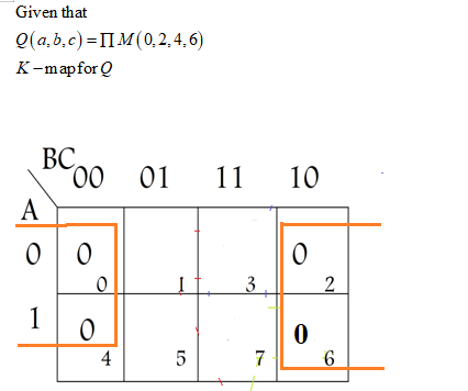
For Q(a,b,c)= NM(0,2,4,6) what is the reduced form of the logic function in POS form? C B'C'+BC' C' (B'+C') .(B+C')


Q: Q3 A: Simplify the following Boolean functions, using Karnaugh maps: F(1,y, 2)- Σ (0,1,4,5 ) Q3 B:…
A: so we need to find the the simplified expression and the logic circuit.
Q: You want to design an arithmetic comparison unified logic circuit. (a) List the steps that you will…
A: 4 bit comparator
Q: I need help with all of them please:)))) Thank you!!
A:
Q: 10 11 12 13 A C 4X1 Q MUX F(A,B,C,D) S1 SO A = MSB D = LSB в D Which of the following is the writing…
A:
Q: Simplify the given expression to its SOP form. Draw the logic circuit for the simplified SOP…
A:
Q: F(A, B, C, D) = E(0, 2, 8, 9, 10, 11, 15) with d(A, B, C, D)= E(4, 6, 12, 13) 1) Given the Boolean…
A:
Q: Use Boolean algebra to simplify the following expression, then draw a logic gate circuit for the…
A: In this question , we will simplify given boolean expression and draw logic gate for simplified…
Q: 2) Design a logic circuit to realize the following Boolean function F(x,y,z) = IIM(0,1, 2, 6, 7) D)…
A: 1.Decoder
Q: Simplify the following Boolean expression after that you will have to draw a logic circuit for the…
A:
Q: Construct the Karnaugh map for the logicfunction defined by the truth table,and find the minimum…
A:
Q: We need a logic circuit that gives a high output if a given hexadecimal digit is 4, 6, C, or E. The…
A:
Q: Q. 1 Derive the minimal SOP expression of f in Figure for Q. 1. Also comput cost of the logic…
A: Given
Q: 3. Design a PLA circuit which realizes the following Boolean functions: (a) Simplify the Boolean…
A:
Q: f(x,y,z,w)= Σ m(0, 2, 5, 8, 10, 12, 14, 15) of function a) Write down the truth table . b) Draw…
A: Given the function F(x,y,z,w)= Σ m(0, 2, 5, 8, 10, 12, 14, 15)
Q: Minimize the following Boolean function use five variables K-map 1. In SOP and draw the logic…
A:
Q: Simplify the given Boolean function in SOP form using K-map F (A,B,C,D,E)…
A: Given ,FA,B,C,D,E=Σm8,9,10,11,13,15,16,18,21,24,25,26,27,30,31
Q: below. Simplify the Boolean expression using Boolean Laws and De Morgan's theorem. Redraw the logic…
A:
Q: 2. A logic function is described by its MINTERMS as the following set: f(A,B,C) = m(1,2,3,5) (a) (b)…
A:
Q: Design a PLA circuit which realizes the following Boolean functions: "check the image" (a) Simplify…
A:
Q: Simplify the following Boolean function F, together with the don't-care conditions d, and then draw…
A: This problem belongs to digital electronics. It is based on the concept of k map simplification.
Q: We need a logic circuit that gives an output X that is high only if a given hexadecimal digit is…
A:
Q: Design a combinational circuit that accepts a 2-bit number (AB) and generates a 5-bit binary number…
A:
Q: Write the Boolean expression from given logic circuit diagram and simplify the output. Please show…
A: The Boolean expression can be obtained by writing the expression across all the gates.
Q: Write the Boolean expression equivalent to the following logic circuit. Do not simplify!
A: Since only boolean expression is asked in the question with no simplification, so solving according…
Q: 2- Derive the POS expression for the following truth table and draw the equivalent logic cct. using…
A: The truth table is as shown below : From the truth table the POS expression is : X =…
Q: Apply Boolean algebra to digital logic circuit analysis A BC DE FG 10 12 13 14 15
A:
Q: Given that a logic ecircuit has the following Boolean expression: F = (A + C)(AB + AC) Convert the…
A: The given Boolean expression is, F=A+CAB+AC
Q: (23) Design the logic circut to the truuth table shown: caresponding C 1. 1.
A:
Q: 4. Given that a logic cireuit has the following Boolesan expression: F= (A + C)(AB + AC) (a) Convert…
A:
Q: Q. Design a circuit which can turn BCD code into both Excess 3 and 2421 code using a single ROM.…
A:
Q: - EXAMPLE : Using the Karnauph Map, find the simplified Boolean expression fo logic expression: Y =…
A: The solution can be achieved as follows.
Q: 1. (a) Implement the following Boolean function with 2n-1 multiplexer. F (A, B, C, D)…
A:
Q: A function F is defined including Don’t Care by: F (A.B, C, D) = Em( 0, 2, 3, 5, 6, 7, 8, 9) +…
A:
Q: f(x, y, z, w) = wz +xz +ãy +wšz a. (5pt) Is the expression in Standart form? If not, express in…
A:
Q: 3. Design a PLA circuit which realizes the following Boolean functions: (a) Simplify the Boolean…
A:
Q: Q (A, B, C) = A̅ .B̅. C +A̅ .B. C + A .B. C̅ + A.B.C Karnaugh function given in the form Using the…
A: Q (A, B, C) = A̅ .B̅. C +A̅ .B. C + A .B. C̅ + A.B.C
Q: a. Construct a Karnaugh map for the logic function F = A ¯ B C ¯ D ¯ +AB C ¯ D ¯ + A ¯ B C ¯ D +AB C…
A: The above function is given as K-map is given as
Q: 3. Design a PLA circuit which realizes the following Boolean functions: (a) Simplify the Boolean…
A:
Q: Digital logic and design.. Please help with a truth table and circuit for ((AB)’(AC’)’)’ Thank…
A:
Q: Convert the boolean expression F = z + xy' to NAND-NAND, and create the resulting logic diagram
A: Given F = z + xy'
Q: . Simplify the Boolean expression AB+(AC)`+AB`C(AB+C) 5. Use the Design Procedure to design a…
A: “Since you have asked multiple questions, we will solve the first question for you. If you want any…
Q: Using Karnaugh maps, find a minimal POS expression for each of the logic function: Y (A, B, C, D) =…
A: From the given equation we can find the sum of product. To find the product of sum we have to fill…
Q: Q6: a) Simplified using P.O.S., then draw logic circuit for your Boolean expression. y(A, B, C, D) =…
A:
Q: Design a logic circuit that satisfy the following Boolean relation. fx + Y= {* + 2 lx +1 when x 5…
A: Given X is a 3-bit binary number and Y is given as, When X is 7, the Y is 8 Hence, Y is a 4-bit…
Q: Given the Boolean function F = A'B (D' + C'D)+ B(A+ A'CD) 3. construct the logic-gate implementation…
A:
Q: Simplify the following Boolean expressions. Then, design the minimized circuits using 7404s, 7408s,…
A:
Q: - Implement a logic circuit to verify the following logic function: F= E 1,2,3,4,5,7,8,12,13|| The…
A: Given Function F = Em ( 1,2,3,4,5,7,8,12,13) the given function is in SOP form let the variables are…
Q: Minimize the following Boolean function use five variables K-map 1. In SOP and draw the logic…
A:
Q: Simplify the following Boolean Expression and Implement the simplified Logic diagram with Truth…
A: Simplifying the diagram,we get,
Q: Using Boolean algebra, simplify the following expression. Then draw the design circuit, write the…
A: To implement the given expression


Step by step
Solved in 2 steps with 1 images


- DIGITAL LOGIC DESIGN Are the following addition results Overflow or underflow and why?Design the following combinational logic circuit with a four-bit input and a three-bit output. The input represents two unsigned 2-bit numbers: A1 A0 and B1 B0. The output C2 C1.C0 is the result of the integer binary division A1 A0/B1 B0 rounded down to three bits. The 3-bit output has a 2-bit unsigned whole part C2 C1 and a fraction part CO. The weight of the fraction bit CO is 21. Note the quotient should be rounded down, i.e. the division 01/11 should give the outputs 00.0 (1/3 rounded down to 0) not 00.1 (1/3 rounded up to 0.5). A result of infinity should be represented as 11.1. A minimal logic implementation is not required. (Hint: start by producing a truth table of your design).Q (A, B, C) = A̅ .B̅. C +A̅ .B. C + A .B. C̅ + A.B.C Karnaugh function given in the form Using the mapping method, you can use the simplified function separately in terms of minterms and maxters. obtain. Output functions with AND NOT for minterms and OR for maxters. Install separately with logic doors.
- Sub:Digtial Logic DesignDesign a 3-bit counter that counts the following sequence: 7,5, 3. 1.0.7, 5. 3, 1, 0, 7. etc. Using the sequential design technique that starts from a state diagram, draw the state table. minimize the logic. and draw the final circuit. The outputs of logic circuit are 2 = Qo Q1. I, = Qo.Qi + Qo.Qi, Io = Qo.Q2, Cont2 = Qj Q2 Cont1 = Qu Q2. Cont0 = Q2 Qo.Q1. h = Qo.Qi + Qo.Q1, Io = Qo Qz Cont2 = Q, Q2 Contl = Qo Q2 Cont0 = Q2 Qo Qı Ij = Qo.Q, + Q».Qı, Io = Qo. Q2. Cont2 = Qj Q2. Contl = Qo.Q2. Cont) = Q2 L = Qo.Qı. I¡ = Q. Qj + Qu Q Io = Qv.Qz Comt2 = Q, Q, Contl = Q Q2 Cont0 = Q2 !! fefsto How much will be per-product cost and thDigital logic design Solve it with drawing and simulation lab I need them both to have the full solution. And thanks Design counter that counts from 00 to 59, using the IC 74LS90 ripple counter and use two 7 segment display to display the result count. You can also use 7447 binary to 7-segment Display Decoder.
- a) Create a 4 Variable Karnaugh Map in paper by mapping 1’s for given standard SOP Boolean expression. After mapping , make relevant groups within Karnaugh Map by considering rules for making groups for 4 variable Karnaugh Map. After making relevant grouping , extract the minimum SOP expression by considering rules for extracting minimum SOP using Karnaugh Map. * Standard SOP: *Create Circuit Diagram using logic gates and logic converter in Multisim for given standard SOP and minimum SOP which you have solved. Do make sure that truth table for both expressions should evaluate same result.Simplify the following expression using Karnaugh map and implement. Draw simplified logic diagram as well. Implement on Multisim software. (a) Y=A.B.C'.D+A.B'.C'.D+A'.B'.C'.D+A'.B.C'.D+A'.B'.C'.D'+A'.B.C'.D'+A'.B.C.D'+A'.B.C.D+A'.B'.C.DAn X-input exclusive-OR gate and a Y-input exclusive-OR gate (where X=3, Y=4 have their outputs connected to a 2-input exclusive-NORgate. Do the following:a) Draw the logic diagram and analyze the logic expression of the output (in standard SOPform).b) List out all essential prime implicants.
- Q (A, B, C) = A̅ .B̅. C +A̅ .B. C + A .B. C̅ + A.B.C Karnaugh function given in the form Using the mapping method, you can use the simplified function separately in terms of minterms and maxterms. obtain. Output functions with AND NOT for minterms and OR for maxters. Install separately with logic doors.2.1 Combinational logic circuits. Tabulates a truth table for the following Boolean expression shown in Equation 1.1. f = A.B.C + A.B.C + A.B.C (1.1) 2.2 Half adder. A half adder is a circuit that adds two binary digits, A and B. It has two outputs, sum (S) and carry (C). The carry signal represents an overflow into the next digit of a multi-digit addition. Figure 1.2 depicted a logic diagram for a half adder. a. derives the Boolean expression for s and c. b. tabulates a truth table for the half adder. Ao Bo Figure 1.2: Half adder os S CFrom the BCD code whose block diagram is given in the figure below, you can find the 7-segment LED display (with common anode) code. Solving combinational logic circuit will be designed. This type of commercially produced decoder is integrated State the features you consider important by researching the circuits. BCD input at the output of the decoder For the 0-9 values of the information information, the following indicator figures will be seen and the values other than these it will be considered arbitrary. Since the 7-segment LED display has a common anode, The logic "0" will be applied to the burned parts. Draw this circuit.