
Related questions
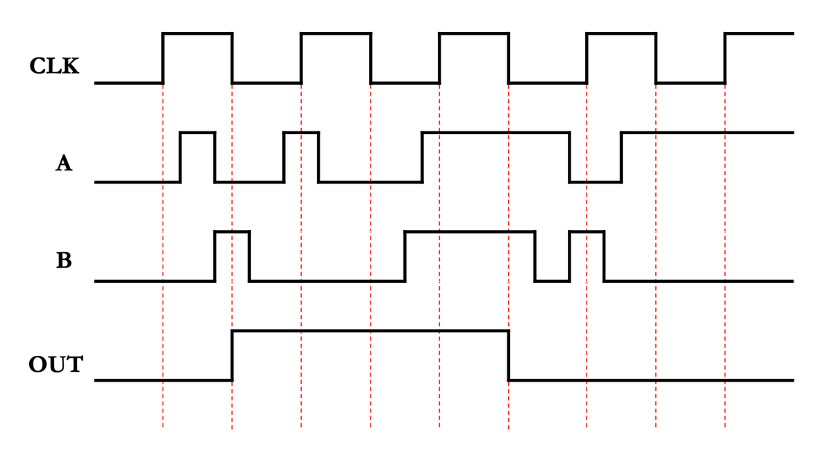
Answer the following questions given the timing diagram of a certain flip-flop which has a clock of 10 MHz and a propagation delay time of 28 ns. Type letters only.
1. What is the type of triggering / clocking used?
A. Positive Level C. Positive Edge
B. Negative Level D. Negative Edge
2. What is the type of flip flop characterized by the timing diagram above?
A. RS NOR Latch C. JK Flip-flop
B. RS NAND Latch D. RS Flip-flop
3. What is the actual input characterized by input “A”?
A. Input “R” C. Input “J”
B. Input “S” D. Input “K”
4. What is the actual input characterized by input “B”?
A. Input “R” C. Input “J”
B. Input “S” D. Input “K”
5. After the circuit’s triggering portion of the clock, how long does it take for the output, OUT, to change state?
A. 1 µs C. 28 ns
B. 0.1 µs D. 128 ns


Trending nowThis is a popular solution!

Step by stepSolved in 2 steps


- The D flip-flop is created by connecting two gated D latches serially, and inverting the CLK input to one of them. The following figure shows the internal circuit of D Flip-flop composing of two latches (L1: Master, and L2: Slave) and NOT gate. Answers the following questions. (Note: You should show all the steps) Complete the truth table below. CLK D CLK1 N1 CLK2 Q Q' 0 0 1 0 0 1 1 1arrow_forwardFigure 2.1 shows the input and the corresponding outputs of a flip-flop whereby QM and Q are taken from the Master latch and the Slave latch respectively. Give the full name of the flip-flop being used here and justify your answers. Use a block diagram for each latch, provide a circuit diagram of the flip-flop you have named. Input QM Q Figure 2.1arrow_forward(a) Complete the following timing diagram for a J-K flip-flop with a falling-edge trigger and asynchronous ClrN and PreN inputs. ClrN Clock ClrN Clock 2₁ PreN (b) Complete the timing diagram for the following circuit. Note that the Ck inputs on the two flip-flops are different. 2₂ J K ClrN li li CLR Ck D₁ Clock li lz CLR Ck D₂arrow_forward
- Computer Networking: A Top-Down Approach (7th Edi...Computer EngineeringISBN:9780133594140Author:James Kurose, Keith RossPublisher:PEARSON
 Computer Organization and Design MIPS Edition, Fi...Computer EngineeringISBN:9780124077263Author:David A. Patterson, John L. HennessyPublisher:Elsevier Science
 Network+ Guide to Networks (MindTap Course List)Computer EngineeringISBN:9781337569330Author:Jill West, Tamara Dean, Jean AndrewsPublisher:Cengage Learning
  Concepts of Database ManagementComputer EngineeringISBN:9781337093422Author:Joy L. Starks, Philip J. Pratt, Mary Z. LastPublisher:Cengage Learning
 Prelude to ProgrammingComputer EngineeringISBN:9780133750423Author:VENIT, StewartPublisher:Pearson Education
 Sc Business Data Communications and Networking, T...Computer EngineeringISBN:9781119368830Author:FITZGERALDPublisher:WILEY