Electric Motor Control
10th Edition
ISBN: 9781133702818
Author: Herman
Publisher: CENGAGE L
expand_more
expand_more
format_list_bulleted
Question

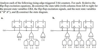
Transcribed Image Text:Analyze each of the following rising-edge-triggered 3-bit counters. For each: 1) derive the
flip-flop excitation equations, 2) construct the state table (with columns from left to right for
the present state variables CBA, the flip-flop excitation signals, and the next state variables
C+B+A+), and 3) construct the state diagram.
a.
CLK
C'
C
B'
B
A'
A
Dc
Da
DA
BA
b.
CLK-
C'
C
B
B
A'
A
To
TB
Fo
CB CA
BA
C'A' CA
CBA C B'A' C'A
BA'
Expert Solution
This question has been solved!
Explore an expertly crafted, step-by-step solution for a thorough understanding of key concepts.
Step by stepSolved in 2 steps with 3 images

Knowledge Booster
Similar questions
- By using the information given in image below design a BCD Counter. You have to provide all the necessary information needed to design this circuit.arrow_forwarddraw nand gate circuit diagram as well,pleasearrow_forwardFlip-flops Give the disadvantages and advantages of Positive Edge Triggering vs Negative Edge Trigerring. Then, give an example of digital circuit and explain where a) Positive Edge is used and b) Negative edge is usedarrow_forward
- a) Design a single-digit decade counter that counts from 0 to 9 and repeats. The single-digit decade counter should be built by a cascaded synchronous binary counter (74LS163) and other basic logic gates. Simulate the complete counter circuit by OrCAD and PSPICE. Capture the circuit schematic and the simulated waveform. (Define the simulation timings for at least one full counting cycle from 0 to 9 and back to 0.) (Hint: Use the DigClock input from the SOURCE as shown below and setup the CLK ONTIME and OFFTIME accordingly for the clock source.) 1/6 Pat DigClock Part List OFFTIME = SuS DSTM1 ONTIME = DELAY= STARTVAL = 0 OPPVAL = 1 Sus EUK FleStim AC Lbrajes Design Cache b) Read the specification of 74LS47 (BCD-to-7-Segment Decoder shown in Appendix) to see how the logic IC operates to drive a 7-segment LED display. Draw the circuit connection of the decade counter in (a) and the decoder to display the count value on the 7-segment LED display. Further explain why common anode…arrow_forwardDesign a 4 bit binary ripple counter that trigger as mention below on the edge of the clock. What will be the count if (a) the normal outputs of the flip‐flops are connected to the clock and that trigger on the positive‐edge of the clock (b) the complement outputs of the flip‐flops are connected to the clock and that trigger on the negative‐edge of the clockarrow_forwardDetermine the Q and Q' output waveforms of the D flip-flop with D and CLK inputs are given in figure (5). Assume that negative edge triggered flip-flop is initially RESET. E, CLK D. 0. 5.arrow_forward
- Q#01: The schematic shown in figure below is for Divide_by_11, a frequency divider, that divides clk by 11 and asserts its output for one cycle. The unit consists of a chain toggle-type flip-flops with additional logic to form an output pulse every 11th pulse of clk. The asynchronous signal rst is active-low and drives Q to 1. Develop and verify a model of Divide_by_11. Vcc 20LSB Q2 03MSB clk clk clk clk clk rst rst rst rst wl w2 clk QB cik_by_11 rst rstarrow_forwardTask 1: Custom Sequence Counter Using JK Flip Flop, Design a counter circuit that cycles through the sequence: 0, 5, 4, 6, 1, 7, and repeats. Follow these steps: a) State Diagram: Draw a state diagram representing the sequence. Each state should be expressed as a binary number. b) State Table: Create a state table for the counter, detailing current states, next states, and outputs. c) Flip-Flop Input Equations: From the state table, derive the input equations for the flip- flops. Treat any unused states as don't-care conditions. d) Simplification using K-maps: Use Karnaugh maps to simplify the flip-flop input equations. Optionally, verify your simplifications using Multisim. e) Circuit Diagram: Draw the circuit diagram. Task 2: 3-bit Up/Down Counter Using Flip Flop of your choice, design a 3-bit counter that counts up or down based on an input signal X. The counter should behave as follows: Initial State: On powerup, the counter starts at 0. Count Up (X=1): Sequence progresses through…arrow_forwardS:41)arrow_forward
- Using synchronous sequential design, detail the steps for the construction of a DECADIC counter operating in the UP/DOWN mode. Taking advantage of the output signals construct a signal that has the duty cycle of 50%. Present the following components: 1.State diagram of the UP/DOWN counter. 2.Transition table from previous state to next state 3.Functions of the J and K signals of each Flip-Flop 4.Circuit timing diagram 5.Circuitry to obtain the output with 50% duty cycle.arrow_forwardA circuit in Figure Q.2a compares 2-bit binary numbers, P and Q represented by PiPo and QiQo respectively. Note that Po and Qo are LSB. (a) Determine under which condition Z will be '1'. (b) Redesign the circuit using active-high 4-to-16 decoder and a logic gate. Z P1 Q1 Figure 2a Po Qo Darrow_forwardA question about 74LS04 IC (a Schmitt Trigger). The pictures show the 74LS04 logic, the connection required and data sheet. Question a)In order to light up the LED, what should Pin 1 and Point A connected to? Ans: Pin 1 connected to (5V / GND), Point A connected to (5V / GND). b)In this example, the power that lights up the LED comes from where? c)What is the current shown on the multi-meter? Is the current flowing out from Pin 2 or flowing into the Pin 2?arrow_forward
arrow_back_ios
SEE MORE QUESTIONS
arrow_forward_ios
Recommended textbooks for you
