
Videos
Consider the circuit shown in Figure P7.23. (a) Write the transfer function
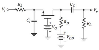
Figure P7.23
a.
The transfer function
Answer to Problem 7.23P
The expression for transfer function of the circuit is,
Explanation of Solution
Given:
The circuit is given as:

Calculation:
Refer to the given circuit:
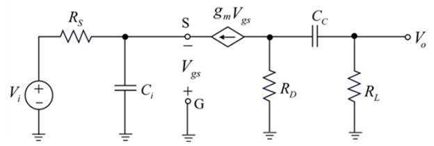
Drawing the small signal equivalent circuit using the simplified hybrid
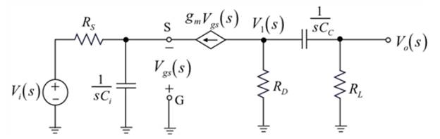
Now drawing the frequency domain equivalent circuit of above figure:
Applying the nodal analysis to derive the expression for
Solving the above equation:
Applying the Kirchhoff s current law at node
Applying the Kirchhoff s current law at output node:
Evaluating the expression for
Substituting
The expression for transfer function of the circuit is given as:
Solving the above equation:
So,
Therefore, the expression for transfer function of the circuit is,
b.
The expression for the time constant associating with the input portion of the circuit.
Answer to Problem 7.23P
The expression of the time constant associated with the input portion of the circuit:
Explanation of Solution
Given:
The circuit is given as:
Calculation:
Evaluating the expression for the time constant associated with the input portion of the circuit.
From the equation (3) , the time constant associated with the input portion of the circuit is,
Hence, the expression of the time constant associated with the input portion of the circuit .
c.
The expression for the time constant associating with the output portion of the circuit.
Answer to Problem 7.23P
The expression of the time constant associated with the output portion of the circuit:
Explanation of Solution
Given:
The circuit is given as:

Calculation:
Evaluating the expression for the time constant associated with the input portion of the circuit.
From equation (3), the time constant associated with the input portion of the circuit is expressed as:
Therefore, the expression for the time constant associated with the output portion of the circuit:
Want to see more full solutions like this?
Chapter 7 Solutions
MICROELECT. CIRCUIT ANALYSIS&DESIGN (LL)


- Problem 7.133(a): For the circuit shown below, let R1 = 106 kN, Rsig = 69 N, and RL Rsig. Assume that %3D 13 kN. Find the value of the bias current I in mA that results in Rin the source provides a small signal vsie and that B = 100. H RL R1 Rsig Ria 8arrow_forwardQ7. For the PMOS common-source circuit shown in Figure P7.69, the transistor parameters are: VTp = -2 V, K, Cgd = 3 pF. (a) Determine the upper 3 dB frequency. (b) What is the equiv- alent Miller capacitance? State any assumptions or approximations that you make. (c) Find the midband voltage gain. 1 mA/V², 1 = 0, Cgs = 15 pF, and +10 V Rs 0.5 kQ R=8 k2 Ci = 2 µF =Cs=10 µF wwHH R;=0.5 k2 Ce2 2 uF R3 = 22 k23 Rp=D 2 k2 RL= 5 k2 -10 V Figure P7.69 19 WW-arrow_forwardA modulating signal f(t) has a maximum frequency of 18 kHz and peak value of 3volt, this signal is encoded using PCM. 1- Calculate the number of bits per sample if the number of levels is 130 2- Calculate the SNRQ if the average power of f(t) is 45 watt. 3- Calculate the minimum system bandwidth. e 7:20arrow_forward
- Does a PCM signal have a smaller bandwidth? Why or Why not?arrow_forwardHow do we get the smal signal model and why CL and Cb doesn’t short the resistance because of the high frequency?arrow_forwardThe relation between Base Current IB, Emitter Current IE and Collector Current IC is Select one: a. IE = IB – IC | b. IB = IC + IE c. IE = IB + IC d. IC = IB + IE %3Darrow_forward
- Q5. In the circuit in Figure P7.65, the transistor parameters are: B = 120, VBE (on) = 0.7 V, VA = 100 V, C, = 1 pF, and fr = 600 MHz. (a) Deter- mine C and the equivalent Miller capacitance CM. State any approxima- tions or assumptions that you make. (b) Find the upper 3 dB frequency and the midband voltage gain. +5 V Rc=4 k2 R = 33 k2 HH Cc2 = 2 µF CCi = 1 µF wwH Rs=2 kQ RL = 5 k2 R2 = 22 kO RE= 4 k2 CE= 10 µF Figure P7.65arrow_forwardA modulated signal with a bandwidth equal to 11.1 KHz. The LSB of the modulated signal is 9.6 KHz and the modulation percentage is fifty-five only. Calculate the following: a. (@.) and (-@.); b.Om; Vm if the amplitude of the LSB is equal to one c. Vc fourth of Vmarrow_forwardQ1. In AM the envelope of the modulated signal waveform is always * .symmetrical around the time axis True False Oarrow_forward
- Bipolar junction transistors (BJTs) are considered “normally-off” devices, because their natural state with no signal applied to the base is no ........... between emitter and collector, like an open switch. * Your answer All field-effect transistors are unipolar rather than bipolar devices. That is, the main current through them is comprised either of ........... through an N-type semiconductor *arrow_forwardDiscuss how the circuit produces a Frequency Modulated Signalarrow_forwardState whether the following statement is true or false. “The curvature in the output voltage of a bandgap reference circuit occurs mainly due to the non-linearity in the PTAT current.”arrow_forward
 Introductory Circuit Analysis (13th Edition)Electrical EngineeringISBN:9780133923605Author:Robert L. BoylestadPublisher:PEARSON
 Delmar's Standard Textbook Of ElectricityElectrical EngineeringISBN:9781337900348Author:Stephen L. HermanPublisher:Cengage Learning
 Programmable Logic ControllersElectrical EngineeringISBN:9780073373843Author:Frank D. PetruzellaPublisher:McGraw-Hill Education
 Fundamentals of Electric CircuitsElectrical EngineeringISBN:9780078028229Author:Charles K Alexander, Matthew SadikuPublisher:McGraw-Hill Education
 Electric Circuits. (11th Edition)Electrical EngineeringISBN:9780134746968Author:James W. Nilsson, Susan RiedelPublisher:PEARSON
 Engineering ElectromagneticsElectrical EngineeringISBN:9780078028151Author:Hayt, William H. (william Hart), Jr, BUCK, John A.Publisher:Mcgraw-hill Education,