
Videos
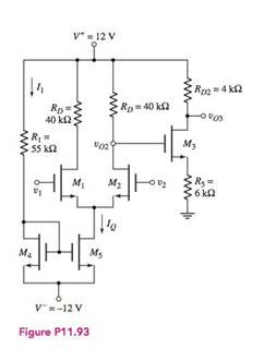
For the transistors in the circuit in Figure
(a)
The values of the differential mode voltage gain and the common mode voltage gain for the given transistor circuit.
Answer to Problem 11.93P
The differential-mode voltage gain is
The common-mode voltage gain is
Explanation of Solution
Given:
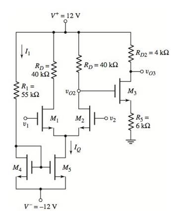
The given circuit is shown below.
The transistor parameters are:
Calculation:
The small signal model of the given transistor circuit is shown below:
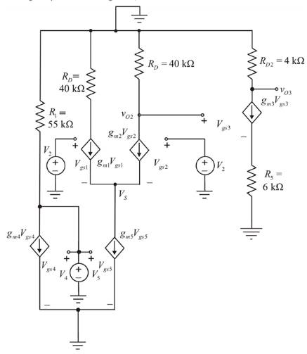
The value of the gate-source voltage of the transistor 4 is calculated as shown below:
The quiescent current is,
The value of the gate-source voltage of the transistor 3 is calculated as shown below:
The transconductance parameters for the differential gain are calculated as shown below:
The differential gain is,
The common mode gain is,
(b)
The values of the output voltage for the given input voltages.
To compare: The result with the ideal case.
Answer to Problem 11.93P
The output voltage is
Explanation of Solution
Given:
The given circuit is shown below.

The circuit parameters are:
Calculation:
The output voltage is calculated as shown below:
On comparing the above output voltage with the ideal case,
Want to see more full solutions like this?
Chapter 11 Solutions
MICROELECT. CIRCUIT ANALYSIS&DESIGN (LL)


- Q1. The output characteristic of a typical transistor is shown below, where the quiescent point is selected on it. This transistor is used in the bias circuit presented below. Find the suitable values of Rg and Rc to fix the Q-point of the circuit properly. +Vcc = 12 V 12- Is = 70 uA 10- Ig = 60 uA 8- Rc Is = 50 uA Rs 6- Ig= 40 uA 4. Is = 30 uĄ Is = 20 uA B = 100 2- VBE = 0.7 V 0- -2- 2 4 6 8 10 12 14 16 VCE (V) Ic (mA)arrow_forward6) the "simplest" model of transistor behavior in this problem, i.e., B = o and IB = 0, with forward bias voltage of AVBE = 0.6V. Consider the following circuit with a transistor and two resistors. You may use 5V a) Determine the output when Vin = 0.5V. 9kN Vout Vin 3002 3kN b) Determine the output when Vin = 1.2 V. c) Determine the output when Vin = 3.6 V.arrow_forwardWhen operated in cutoff and saturation, the transistor acts like a) A linear amplifier b) A switch c) A variable capacitor d) A variable resistor The average output value of half wave rectified voltage with a peak input of 200V is equal to (assume silicon diode) a) 63.66 V b) 127.32 V c) 63.47 V d) 127.101 V The term "Bipolar" in Bipolar Junction Transistor (BJT) refers to a) Two junctions b) Two Diodes c) Two polarity carriers (electrons & holes) d) Two resistancesarrow_forward
- A base current of 50µA is applied to the transistor in the given figure , and a voltage of 5V is dropped across Rc. Determine the Boc of the transistor. Rc 1.0 kn Vcc 100 kn VBBarrow_forwardDetermine the ac parameters for this BJT circuit. Note: DC biasing voltages and currents need to be computed FIRST before calculating the AC parameters of gains and impedances 80 mV HI +10 V R₁ 18 ΚΩ R₂ > 4.7 ΚΩ Rc • 1.5 ΚΩ hFE = 30 hfe = 200 RE * 1.2 ΚΩ CE RL > 5.1 ΚΩarrow_forward11. Determine and draw the resulting output waveform in relation to the inputs for following circuit block. Assume Q starts low. SO R0 Q S D R earrow_forward
- 5V B OV OV For all the MOSFETS assume Vth=1V and k =50 mA/V² R₁ = 4700 Ao M₁ M₂ B Indicate and verify the state of each MOSFET and Vo for the following input combinations. Fill out the table for each assumed state of the MOSFET for every input combination. Use Rds(on) approximation for linear operation and three significant figures for the voltages. M1 is assumed to be in saturation. If Vgs = 2 V, Vds = 4V, Vds > Vgs - Vth 4>2-1 4> 1 (ok) Vgs > Vth (2>1) A M2 state M3 state V. 0 OV 5 V R₂ = 560Ω 5V M1 state M3arrow_forwardDraw the small signal equivalent circuit. Determine the following: Zo Zin Av (voltage gain) Ai (current gain) Voarrow_forwardUsing LTSpice, simulate the circuit below, use 2N3904 for the transistor. Connect the circuit and apply an AC signal at the input with an amplitude of 1mV and a frequency of 1kHz. Determine the Voltage gain of the circuit by dividing Vo with Vin.arrow_forward
- Vec Re Veut Rin Reut R R Venarrow_forwardFrom the circuit below, determine the output peak voltage Vm ? Np:Ns 6:1 Vp 120 Vac out 60 Hz DA R = 200 2 O Ovpeak O 169.71Vpeak O 28.28Vpeak O 1018.23Vpeakarrow_forwardYou can find answers, choose true / false, and then correct the error 1. The quiescent power dissipation occurs when the maximum signal is applied. 2. Efficiency is the ratio of output signal power to total power. 3. Each transistor in a class B amplifier conducts for the entire input cycle. 4. A current mirror is implemented with a laser diode. 5. Darlington transistors can be used to increase the input resistance of a class AB amplifier. 6. The output of a class C amplifier is a replica of the input signal.arrow_forward
 Introductory Circuit Analysis (13th Edition)Electrical EngineeringISBN:9780133923605Author:Robert L. BoylestadPublisher:PEARSON
 Delmar's Standard Textbook Of ElectricityElectrical EngineeringISBN:9781337900348Author:Stephen L. HermanPublisher:Cengage Learning
 Programmable Logic ControllersElectrical EngineeringISBN:9780073373843Author:Frank D. PetruzellaPublisher:McGraw-Hill Education
 Fundamentals of Electric CircuitsElectrical EngineeringISBN:9780078028229Author:Charles K Alexander, Matthew SadikuPublisher:McGraw-Hill Education
 Electric Circuits. (11th Edition)Electrical EngineeringISBN:9780134746968Author:James W. Nilsson, Susan RiedelPublisher:PEARSON
 Engineering ElectromagneticsElectrical EngineeringISBN:9780078028151Author:Hayt, William H. (william Hart), Jr, BUCK, John A.Publisher:Mcgraw-hill Education,