
Videos
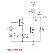
The BiCMOS circuit shown in Figure P11.82 is equivalent to a pnp bipolar transistor with an infinite input impedance. The bias current is
(a)
To sketch: The small-signal equivalent circuit of the given BiCMOS circuit.
Answer to Problem 11.82P
The required sketch is shown in Figure 3.
Explanation of Solution
Given:
The given diagram is shown below.

Calculation:
Mark the value and redraw the circuit.
The required diagram is shown in Figure 1
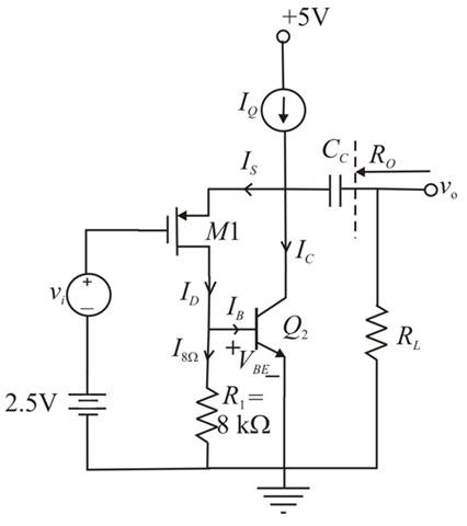
Figure 1
The small signal equivalent circuit is shown in Figure 2
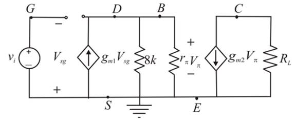
Figure 2
Conclusion:
Therefore, the required sketch is shown in Figure 2
(b)
The small signal parameters for each of the transistor.
Answer to Problem 11.82P
The value of small signal parameters are
Explanation of Solution
iven:
The given diagram is shown below.
Calculation:
The value of the current through the resistance
The expression for the resistance
Substitute
The value of the drain current is calculated as,
The expression for the collector current is given by,
Substitute
The value of the base current is calculated as,
The transconductance of the first transistor is given by,
Substitute
The transconductance of the first transistor is given by,
Substitute
The value of the resistance
Conclusion:
Therefore, the value of small signal parameters are
(c)
The value of small signal voltage gain for the given values of load resistor.
Answer to Problem 11.82P
The value of the small signal voltage gain for
Explanation of Solution
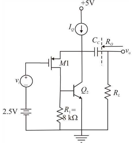
Given:
The given diagram is shown below.

The given values of load resistor is
Calculation:
The expression for the voltage
The expression for the gate to source voltage is given by,
The expression to determine the value of the output voltage is given by,
Substitute
Substitute
Conclusion:
Therefore, the value of the small signal voltage gain for
Want to see more full solutions like this?
Chapter 11 Solutions
MICROELECT. CIRCUIT ANALYSIS&DESIGN (LL)


- QUESTION 6: Consider the circuit of Figure P11.3 with transistor parameters ß= 155 , V4=0, and VBE(on) = 0.66 V. The circuit is biased by V*= 6 V and V = -6 V. Design the circuit such that the Q-point values are Icı = Ic2 = 140 µA, and vo1 =vo2 = 1.2 V for vị = v2 = 0. Format : 98.34 Rc (kN) Format : 47.93 RE (kN) Ici RC RC v02 10a RE Figure P11.3arrow_forwardMost of the following statements about integrated circuits arecorrect, but one is not. Which statement is NOT true? Select one: a. Transistors are constructed in a small area of an integrated circuit,and are connected to other transistors by wires that are embedded inthe integrated circuit b. Wires that carry signals may be embedded in a substrate without a shortcircuit because a short circuit would require a signal to cross areverse biased junction c. Each transistor on an integrated circuit is manufactured individually,one at a time d. An integrated circuit contains several layersarrow_forward2) Consider the circuit given below. (Assume: K-4mA/V', Vt=-1V, A=0, (K= µCox.(W/L)) da Perform DC analysis and calculate Va. Vsg, Vs, voltages, and Ip, gm, ro values bo Draw a small-signal equivalent circuit Co Calculate Av, Rin, Rout values as shown on the schematic Also ) satwaton mode Test for Fill inthe table VG VSG O2m A Rin Vs QUin ID vo Coo 9m Ro Av Rout Rin Routarrow_forward
- A MOSFET with k = 4.5 mA/V2 and VT = 3 V is used in the biasing circuit below. Determine the value of VGS. Options: (a) 0 V (b) 3 V (c) 6 V (d) 4.5 Varrow_forward(b) Draw the ID - VD curves for this MOSFET for ±VD for V₁ = 0 and V₁ = 1 V. VȚ = 1V. n V₁ + p-type D ID V₁arrow_forwardThis problem is AC analysis problem. DC analysis is not needed to answer the question. A) If we assume that the peak voltage of Vbe must be less than 10 mV to avoid small signal violations determine the value of Rsig if Vi has a peak amplitude of 1 V and Is = 1mA. Hint: Don't forget r!! Answer: Rsig =. B) If you did the DC analysis on this problem and calculated Vc = 50 mV and Vs = -100 mV what is the maximum amplitude of the output voltage while the circuit stays in active mode. Answer: Vo,max =, When you "verify" a mode of operation you will need to calculate all three voltages (Vc, Ve, VE for BJTS and VG, Vs, Vp for MOSFETS) and show the correct two conditions are satisfied. Assume Capacitors acts like open circuits at DC and short circuits for AC. > Assume the following: 5V o Beta = 100 O VBE = 0.7 o V: (Thermal) = 26 mV o Vr (Threshold) = 2V O VA = - o For MOSFET saturation mode: assume: lp = K(VGs-Vr)? (Assume K = 10 mA/V²). 5kn C2 01 C1 Rsig 1kn 10k Vi IIs :C3 1mA -5Varrow_forward
- (ii) Calculate the RB, Rc, and the minimum power rating of the transistor (Note: the actual power rating should be greater).arrow_forwardPrelab: Using the BJT large signal model for the circuit in Figure 1, determine the Vub voltage required to drive a collector current of I, = 0.5 mA. Use RB = 220 kN, Rc = 2.05 kN, RE = 1.05 kN, and Vee = 5V. Assume Is = 50nA and ß = 250. (Hint: Find Vbe using Ic, then use KVL to find Vbb, remember that Ib can be found using the Ic/ ß relationship) RC Voc R3 bb RE Figure 1 NPN BJT under DC Biasarrow_forwardWhat is the output resistance of this circuit in units of ohms? All of the transistors are n-type MOSFETs with kp=0.05 and lambda=0.1. The two DC biasing voltages (Vbias1 and Vbias2) are set to create a current through M3 of 2 mA, current through M2 of 1 mA, and current through M1 of 1 mA. (Hint: Rout is not 10000.)arrow_forward
- Coonsider the common emitter amplifier shown in figure below. Assume a β of 100, VBE = 0.7V, VT = 25mA and VA = 100V. Draw an equivalent DC model and determine the rπ, transconductance (gm) and ro. Draw an equaivalent AC model using the small-signal model Find an expression for vbe and vo in terms of the input voltagearrow_forwardFrom the figure shown, when S1 is at 1 : up position; the following statement is not correct except: (a) Collector-emitter voltage of Q1 is approximately zero (b) the LED will illuminate (c) the base voltage of Q2 is equal to 9 V (d) (b) and (c)arrow_forwardConsider the circuit of Figure 12.7 on page 605. Given VCC=10 V and RC=2 kΩ, construct the load line on the iC versus vCE axes. Repeat for VCC = 15 V. How does the slope of the load line change when VCC changes?arrow_forward
 Introductory Circuit Analysis (13th Edition)Electrical EngineeringISBN:9780133923605Author:Robert L. BoylestadPublisher:PEARSON
 Delmar's Standard Textbook Of ElectricityElectrical EngineeringISBN:9781337900348Author:Stephen L. HermanPublisher:Cengage Learning
 Programmable Logic ControllersElectrical EngineeringISBN:9780073373843Author:Frank D. PetruzellaPublisher:McGraw-Hill Education
 Fundamentals of Electric CircuitsElectrical EngineeringISBN:9780078028229Author:Charles K Alexander, Matthew SadikuPublisher:McGraw-Hill Education
 Electric Circuits. (11th Edition)Electrical EngineeringISBN:9780134746968Author:James W. Nilsson, Susan RiedelPublisher:PEARSON
 Engineering ElectromagneticsElectrical EngineeringISBN:9780078028151Author:Hayt, William H. (william Hart), Jr, BUCK, John A.Publisher:Mcgraw-hill Education,