
a.
The width to length ratio of the transistors to meet the requirements.
a.
Answer to Problem 3.47P
Explanation of Solution
Given Information:
The given values are:
The given circuit is shown below.
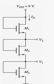
Calculation:
The voltage is,
Also,
And,
Then the constant current is
Similarly,
And,
b.
The change in the output voltages for the
b.
Answer to Problem 3.47P
When
When
Explanation of Solution
Given Information:
The given values are:
The given circuit is shown below.
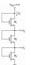
Parameter
Calculation:
When there is a change in
From part (a),
For each case,
Then,
Also,
Substituting equation (1)
From equation (1),
So,
When
When
c.
The output voltages for a specified change in each transistor.
c.
Answer to Problem 3.47P
Explanation of Solution
Given Information:
The given values are:
The given circuit is shown below.
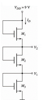
Also,
Calculation:
When there is a change in
For M1 :
Now for M2 and M3 :
From part(a),
Then,
Also,
Substituting equation (1)
From equation (1),
Want to see more full solutions like this?
Chapter 3 Solutions
Microelectronics: Circuit Analysis and Design

- Q1) Answer True or False for the following: 1- Field-effect transistors are Bipolar devices. 2- A depletion MOSFET (D-MOSFET) can operate with a zero, positive, or negative gate-to source voltage. 3- The 4-layer diode is a thyristor that conducts when the voltage across its terminals exceeds the breakover potential. 4- The benefit of SCR Crowbar is power amplification. 5- Most op-amps require only a positive dc supply voltage.arrow_forwardFor the circuit shown find: a. Power consumed in RL b. DC voltage of current source Ip dc. c. Q points of operation of the 2 transistors If it is not possible to calculate explain by laws. ID = 3 milliamperes. All semiconductors are silicon. Vcc 12 V BETA=100 ID Q1 D1 D2 Q2 100 Q D, 10 k2 VEE - 12 Varrow_forwardAn npn transistor has the CE input characteristics shown in Figure 3-19 (p. 115) and the CE output characteristics shown in Figure 3-20 (p. 115). (a) Find IB when VBE = 0.7 V and VCE = 20 V. (b) Find the beta of the transistor at VCE = 6.0 V and IB = 20uA (neglecting leakage). (c) Find bac for VCE = 6.0V and IB varying from 20 uA to 40 uA. (d) What is the approximate value of VCE,sat in Fig. 3-20?arrow_forward
- A transistor has the CB input characteristics shown in Figure 3–11 (p. 106 ). If alpha = 0.95, find IC when VBE = 0.72 V and VCB = 10 V.arrow_forward3. Write down which transistor structure each curve characteristic belongs to in the figure. Ip -VGS -VGS +VGs (c) VGS (b) (a)arrow_forwardFor the PN junction under sun light, the short circuit current amount is Isc. Please sketch the I-V curve of PN under the sun based on that under the dark condition above. Indicate Isc and Voc in your plot.arrow_forward
- TransistorsFill in the blanks with the words below:amplify, bipolar transistor, current, device, embedded, field, field-effect transistor, fundamental,implemented, milestones, standardized, terminals, ubiquitous, vacuum tube, voltageA transistor is a semiconductor 1……….. used to amplify or switch electronic signals and electrical power. It iscomposed of semiconductor material usually with at least three 2 …………. for connection to an external circuit. A3. ………… or current applied to one pair of the transistor's terminals controls the current through another pair ofterminals. Because the controlled (output) power can be higher than the controlling (input) power, a transistor can4 …………… a signal. Today, some transistors are packaged individually, but many more are found 5 …………. inintegrated circuits.The transistor is the 6 …………. building block of modern electronic devices, and is 7. …………in modern electronicsystems. Julius Edgar Lilienfeld patented a 8 …………….. in 1926 but it was not…arrow_forwardQ2 Design a voltage divider bias circuit for an npn silicon transistor having B = 100 to be used in a Common Emitter configuration. The quiescent point (Q point) is to be lc = 1 mA, VE = 5 V. The supply voltage (Vcc) is 15 V. Assume VĘ = 0.1Vc and BRĘ 2 10R2. (a)Find all the resistors values and draw the schematic diagram of this Common Emitter Amplifier with bypass capacitor Cę.arrow_forwardA simple diode rectifier has 'ripples' in the output wave which makes it unsuitable as a DC source. To overcome this one can use a capacitor in series with a the load resistance. Select one: O True O False Fixed bias is less stable than Voltage divider bias in transistor biasing techniques. Select one: O True O Falsearrow_forward
- The junction between the base and collector of a transistor is called: O a. Collector Junction O b. Source Junction O c. Emitter Junction d. Base Junctionarrow_forwardWhich of the following is a type of Metal Oxide Semiconductor Field Effect Transistor: O P channel JFET O None of them O N channel D- MOSFET in O N channel JFET A simple diode rectifier has 'ripples in the output wave which makes it unsuitable as a DC source. To overcome this one can use of a capacitor in series with a the load resistance. stion Select one: O True O Falsearrow_forwardRefer to section 3.5.3 in your textbook that deals with a bridge rectifier. If the input signal is a sinewave with amplitude = 10V & freq = 1KHZ, RL=1KN and VD=0.4V. a) Proof that the average value of the output voltage = V, – 2Vp, then determine its numerical value. b) Derive an expression for the peak diode current, then determine its numerical value. VISINarrow_forward
 Introductory Circuit Analysis (13th Edition)Electrical EngineeringISBN:9780133923605Author:Robert L. BoylestadPublisher:PEARSON
 Delmar's Standard Textbook Of ElectricityElectrical EngineeringISBN:9781337900348Author:Stephen L. HermanPublisher:Cengage Learning
 Programmable Logic ControllersElectrical EngineeringISBN:9780073373843Author:Frank D. PetruzellaPublisher:McGraw-Hill Education
 Fundamentals of Electric CircuitsElectrical EngineeringISBN:9780078028229Author:Charles K Alexander, Matthew SadikuPublisher:McGraw-Hill Education
 Electric Circuits. (11th Edition)Electrical EngineeringISBN:9780134746968Author:James W. Nilsson, Susan RiedelPublisher:PEARSON
 Engineering ElectromagneticsElectrical EngineeringISBN:9780078028151Author:Hayt, William H. (william Hart), Jr, BUCK, John A.Publisher:Mcgraw-hill Education,