
Videos
Consider the NMOS circuit shown in Figure 3.36. Plot the voltage transfer characteristics, using a PSpice simulation. Use transistor parameters similar to those in Example 3.9. What are the values of
To plot: Thevoltage transfer characteristics using PSpice simulation.
To find: The value of output voltage for the given input voltage.
Answer to Problem 3.3CAE
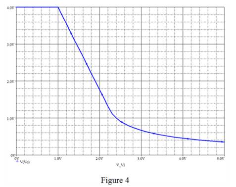
The required plot is shown in Figure 4 and the output voltage for the input voltage of
Explanation of Solution
Given:
The required diagram with the values marked is shown in Figure 1.
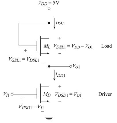
Figure 1
Calculation:
Draw the PSpice equivalent circuit with all the values marked.
The snip for the drop box with all the setting is shown in Figure 3

Left click on the trace option and then click on add trace and type “V(Vo)”command in trace expression box to obtain the voltage transfer characteristic of the inverter.
The required characteristic diagram is shown in Figure 4
Consider the input voltage is
The expression for the current
The expression for the current
The expression for the value of the voltage
The expression for the current
Substitute
Substitute
The input voltage is just
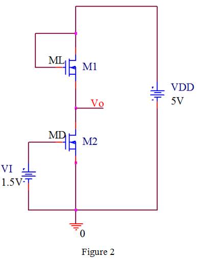
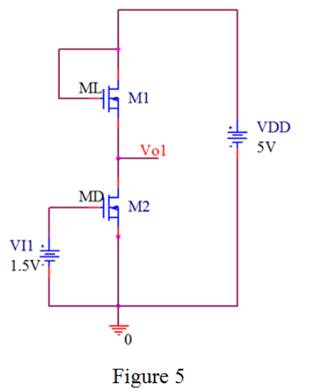
Draw the PSpice circuit for the figure 1 with the input voltage of
The required diagram is shown in Figure 5
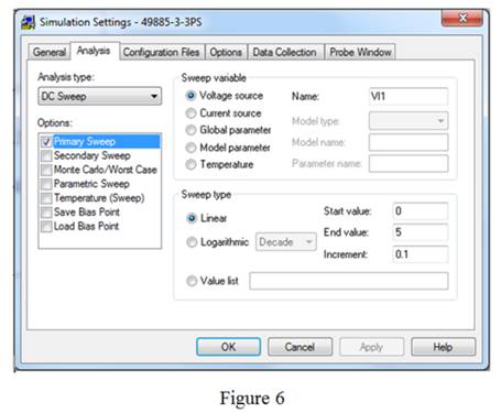
The simulation settings for the circuit is shown in Figure 6
The simulated circuit for Figure 5 with the output voltage is shown in Figure 7
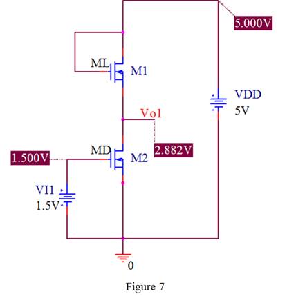
Thus, the value of the simulated output voltage is same as the theoretical output voltage.
Consider the input voltage is
Mark the values and draw the circuit for the input voltage of
The required diagram is shown in Figure 8
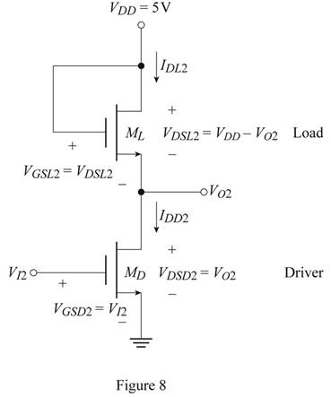
The values of different voltage are,
The driver transistor is biased in non-saturation region as the drain to source voltage is very large. So the expression for the relation of the drain currents is given by,
The expression for
The load transistor is in the saturation region and the drain current is given by,
By the relation
The value of the output voltage is evaluated as,
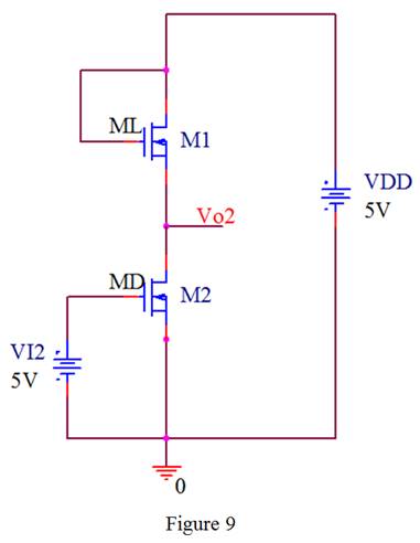
The simulation circuit for Figure 8 is shown in Figure 9
The output of the simulated circuit for the above circuit is shown in Figure 11
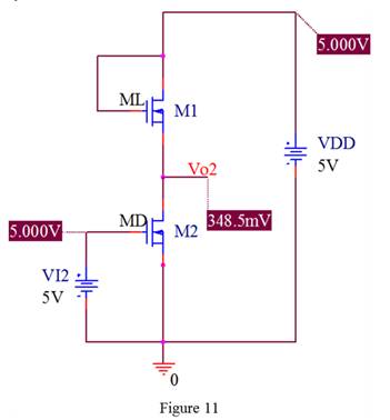
Thus, the output voltage of
Conclusion:
Therefore, the required plot is shown in Figure 4 and the output voltage for the input voltage of
Want to see more full solutions like this?
Chapter 3 Solutions
Microelectronics: Circuit Analysis and Design


- a) Figure B3 shows a cross section for a Metal Oxide Semiconductor Field Effect Transistor (MOSFET) in diagrammatic form. (i) (ii) Sketch the energy band diagram for the MOSFET along the line X-Y shown in Figure B3 when bias voltages are applied such that the silicon surface is inverted. Label all important features of your sketch and state any assumptions made. Sketch a box plot showing the charges present in the structure when the silicon surface is inverted. Indicate the source of all the charges and state whether they are positive or negative. Source n+ Metal Silicon Substrate - p X dioxide Drain n*arrow_forward• In MOSFET, it is the foundation upon which the device will be constructed and is formed from a silicon base A. Substrate, B. Slab, C. Source, D. Base.arrow_forwardAn integrated circuit or monolithic integrated circuit (also referred to as an IC, a chip, or amicrochip) is a set of 1.................. on one small flat piece (or "chip") of semiconductor material,normally 2. ……………The integration of large numbers of tiny transistors into a small chip results in circuits that areorders of magnitude smaller, cheaper, and faster than those constructed of discrete electroniccomponents. The IC's mass production 3. ………….., reliability and building-block approach tocircuit design has ensured the rapid 4…………. of standardized ICs in place of designs usingdiscrete transistors. ICs are now used in virtually all electronic equipment and haverevolutionized the world of electronics. Computers, mobile phones, and other digital homeappliances are now 5. ………….. parts of the structure of modern societies, made possible by thesmall size and low cost of ICs. Integrated circuits were made practical by mid-20th-century technology 6. …………….…arrow_forward
- The mode of operation for the D-MOSFET is Select one: a. the ohmic region only b. the enhancement mode only c. both the depletion and enhancement modes d. the depletion mode onlyarrow_forwardExplain the operation and Analyse the performance of a range of discrete semiconductor devices used in modern electronic systems in terms of simple semiconductor theory, and suggesting appropriate applications for each, such as: Triac. • MOSFET. Thyristors.arrow_forwardb) For the transistor small signal h-parameter equivalent circuit shown in figure Q3b write down equations for Vbe and Ic in terms of Ib and Vce. hie Ie Vbe hreVce (+ hfelb 1/hoe Vce Figure Q3barrow_forward
- 1. For a certain D-MOSFET, IDSS = 18 mA, and VGS = +10V. Vp =4V. a) Determine ID at VGS =+ 3V. b) Determine ID at VGS = -3V. %3Darrow_forwardQ1: for a silicon transistor in the figure below = 200 dc {What is the voltage between the collector and emitter VCE, drawing the load line and finding the Q pointarrow_forward2. We discussed in class how the channel capacitance can be modeled in different region of operations in MOSFETs. For your reference, the slide is shown below. Explain how you think the model would look like if a transistor is in velocity saturation region? Channel Capacitances Channel capacitance is a voltage dependent and non-linear capacitance S C P-sub Bulk Cutoff Region D Operation Region Cutoff Linear Saturation S P-sub Bulk C Linear Region CGBCH CoxWLeff 0 0 1 2 3 S P-sub Bulk Saturation Region CGSCH 0 сат CoxWL eff 1 2 CGDCH 0 CoxWLoft CoxWLoff eff D 0arrow_forward
- For the PN junction under sun light, the short circuit current amount is Isc. Please sketch the I-V curve of PN under the sun based on that under the dark condition above. Indicate Isc and Voc in your plot.arrow_forwardA transistor has the CB input characteristics shown in Figure 3–11 (p. 106 ). If alpha = 0.95, find IC when VBE = 0.72 V and VCB = 10 V.arrow_forwarda) What is a Field effect transistor? Give its description and classification.b) Explain the working of n-channel / p-channel Junction Field EffectTransistor with its drain characteristics.arrow_forward
 Introductory Circuit Analysis (13th Edition)Electrical EngineeringISBN:9780133923605Author:Robert L. BoylestadPublisher:PEARSON
 Delmar's Standard Textbook Of ElectricityElectrical EngineeringISBN:9781337900348Author:Stephen L. HermanPublisher:Cengage Learning
 Programmable Logic ControllersElectrical EngineeringISBN:9780073373843Author:Frank D. PetruzellaPublisher:McGraw-Hill Education
 Fundamentals of Electric CircuitsElectrical EngineeringISBN:9780078028229Author:Charles K Alexander, Matthew SadikuPublisher:McGraw-Hill Education
 Electric Circuits. (11th Edition)Electrical EngineeringISBN:9780134746968Author:James W. Nilsson, Susan RiedelPublisher:PEARSON
 Engineering ElectromagneticsElectrical EngineeringISBN:9780078028151Author:Hayt, William H. (william Hart), Jr, BUCK, John A.Publisher:Mcgraw-hill Education,