
Concept explainers
(a)
The value of the collector current, base current and the node voltages for the given values.
(a)
Answer to Problem 17.38P
The value of the base voltage
Explanation of Solution
Calculation:
The given diagram is shown in Figure 1
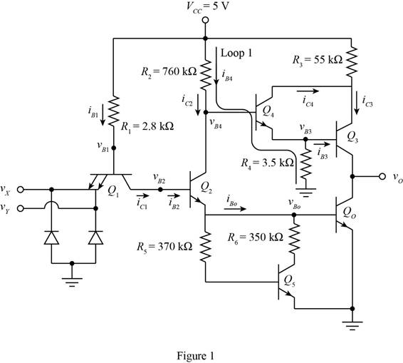
The expression for the voltage
Substitute
The expression for the base current of the first transistor is given by,
Substitute
The expression for the voltage
Substitute
The first transistor are forward biased and the other transistor are operating in the cut off region therefore the value of the different collector current is given by,
The expression for the current
The conversion from
The conversion from
The expression for the value of the current
Substitute
The expression for the value of the current
Substitute
The expression for the base voltage of the fourth transistor is given by,
Substitute
Conclusion:
Therefore, the value of the base voltage
(b)
The value of the collector current, base current and the node voltages for the given value.
(b)
Answer to Problem 17.38P
The value of the base voltage
Explanation of Solution
Calculation:
The expression for the value of voltage
Substitute
The expression for the base current of the first transistor is given by,
Substitute
The expression for the voltage
Substitute
The expression for the value of the second transistor is given by,
Substitute
The expression for the value of the current
Substitute
The expression for the voltage
Substitute
The expression for the value of the current
Substitute
The expression for the value of the voltage
The expression for the value of the current
The expression for the value of the current
The expression for the value of the voltage
Substitute
The expression for the value of the current
Substitute
The expression for the value of the current
Substitute
Conclusion:
Therefore, the value of the base voltage
Want to see more full solutions like this?
Chapter 17 Solutions
Microelectronics: Circuit Analysis and Design


- 2. What is the function of internal transistor T1 in the IC 555? What main advantages do you think the Pulse width modulated signal has over Pulse Amplitude Modulated signal? 3. What is the reason for the error which is inevitably present on the PW demodulated signal? 4.arrow_forwardQ7: An analog signal is quantized and transmitted by using PCM system. If each sample at the receiving end of the system must be within ± 0.5 percent of the peak -to-peak full-scale value. How many binary digits must each sample contain? Ans: 7.arrow_forward-Design ADC using VTC (Voltage to Time Converter) with clock generator fe=32Hz and the slope of voltage to time converter K= 0.025 and the maximum analog input VA-20V, find 1- Number of bits to design the counter 2- The digital conversion (Binary form) of analog input-17.3V 3- Total conversion time.arrow_forward
- Q. Consider the following non-matched CMOS inverter shown in the figure with Vtn=-Vtp=0.4 V, and Kn=0.3mA/V?, and Kp=1.5mA/V? VDD ipp ס ןשarrow_forwardintegrated circuit families (RTL, DTL, TTL, CMOS) 4. Let vx = vy = 0.1V (Logic 0), B = 25 Determine all the currents and voltages in the circuit below: 11, 12, iR, IRC, iB, v1 & vo. Vcc=5 V 84 48 = 4 ΚΩ VI Dx vx H Vy O KH Dy RB = 10 ΚΩ Figure 17.20 Basic diode-transistor logic gate D₁ D2₂ DA IRC VB ≤RC= 14 ΚΩ -OVO loarrow_forward1. A) An 8-bit ADC with a reference voltage of 5V is implemented using the Counter Ramp technique. Assume the input voltage is 1.4V. How many clocks are needed to conduct a conversion? You do not need consider the sampling time. B) A 10-bit ADC with a reference voltage of 5V is implemented using the SAR technique. Assume the input voltage is 3.2V. How many clocks are needed to conduct a conversion? You do not need consider the sampling time. C) An analog signal has a maximum frequency of 300HZ, what should be the minimum sampling rate of the ADC so that the digitized data can be used to perfectly reconstruct the original analog signal? D) For an 8-bit DAC, if Vref = 6 V, and the input code is 0×4B (01001011), what is the DAC output voltage? E) A 8-bit ADC has a reference voltage of 6V. What is the max quantization error?arrow_forward
- HW.3 1-Design a 4 bit Flash ADC. With Vref = 10 V and Vin=4.1V. 2-Find the operation diagram for a 4 bit successive - approximation converter ADCarrow_forward3. Design an SCR circuit that could give a 75⁰ degrees conduction angle and 105⁰ firing delay angle. Consider the importance of the parameters and include your computation.arrow_forward8 Draw the block diagram of a Phase Locked Loop used as an Integer N frequency synthesizer. If the output is taken from the output of the VCO, what do we get. Briefly explain the different modes of operation of a PLL. Comment which mode of operation is the largest one. Name one application of PLL other than the ones discussed above.arrow_forward
- 3/ An analog signal is converted to a binary PCM signal and transmitted over a band-limited channel at 100 kHz. band-limited channel at 100 kHz. Thirty-two quantization levels are used. a/ Calculate the maximum bit rate that can be transmitted. b/ Calculate what is the maximum bandwidth that the analog signal can have.arrow_forwardWrite an HDL behavioral description of a BCD-to-excess-3 converter.arrow_forwardBriefly describe Register Transfer Structure in RTL.arrow_forward
 Introductory Circuit Analysis (13th Edition)Electrical EngineeringISBN:9780133923605Author:Robert L. BoylestadPublisher:PEARSON
 Delmar's Standard Textbook Of ElectricityElectrical EngineeringISBN:9781337900348Author:Stephen L. HermanPublisher:Cengage Learning
 Programmable Logic ControllersElectrical EngineeringISBN:9780073373843Author:Frank D. PetruzellaPublisher:McGraw-Hill Education
 Fundamentals of Electric CircuitsElectrical EngineeringISBN:9780078028229Author:Charles K Alexander, Matthew SadikuPublisher:McGraw-Hill Education
 Electric Circuits. (11th Edition)Electrical EngineeringISBN:9780134746968Author:James W. Nilsson, Susan RiedelPublisher:PEARSON
 Engineering ElectromagneticsElectrical EngineeringISBN:9780078028151Author:Hayt, William H. (william Hart), Jr, BUCK, John A.Publisher:Mcgraw-hill Education,