
Concept explainers
(a)
The value of the current
(a)
Answer to Problem 17.11EP
The value of the current
Explanation of Solution
Calculation:
The given diagram is shown in Figure 1
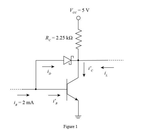
Apply KVL in the above circuit.
Substitute
The expression for the value of the current
Substitute
The expression for the value of the base current
Substitute
The expression for the value of the drain current is given by,
Substitute
(b)
The value of the current
(b)
Answer to Problem 17.11EP
The value of the current
Explanation of Solution
Calculation:
Apply KVL in the above circuit.
Substitute
The expression for the value of the current
The expression for the value of the current
The expression for the value of the current
From equation (2) and equation (3), the value of the current
Substitute
Substitute
Substitute
Substitute
The expression for the value of the drain current is given by,
Substitute
Conclusion:
Therefore, the value of the current
(c)
The value of the maximum load current.
(c)
Answer to Problem 17.11EP
The maximum value of the load current is
Explanation of Solution
Calculation:
The expression for the value of the
Substitute
The expression for condition of the edge saturation is given by,
Substitute
Substitute
The expression for the value of the load current is given by,
Substitute
Conclusion:
Therefore, the maximum value of the load current is
Want to see more full solutions like this?
Chapter 17 Solutions
Microelectronics: Circuit Analysis and Design


- Determine the folowing A.base current (IB), B. collector current (Ic), C. collector-to-emitter voltage (VCE),D. draw the load line, locate the Q-pointF. input impedance (Zi),G. Output impedance (Zo)arrow_forward3. Design an SCR circuit that could give a 75⁰ degrees conduction angle and 105⁰ firing delay angle. Consider the importance of the parameters and include your computation.arrow_forwardSoru 7 ID(sat.) is 0.0001 A (100 microA) for, and VG =6V for a long channel n-MOSFET with V= 1V. Calculate the saturation current ID(sat.)in units of microA if VG-VT=3V.arrow_forward
- 10. Draw the A.C load-line. 11. Sketch the D.C and A.C voltage at the following point a) The base Scanned by TapScanner b) Emitter c) Collector before and after C-arrow_forwardQ16.Determine the Q point of the transistor circuit shown in the figure. Also draw the d.c. load line. Given β = 200 and VBE = 0.7V.arrow_forwardb) Consider a MOSFET circuit with transistor parameters VTN=0.8V, KN=0.85 mAV and A=0.02V1. i) Determine Rs and Ro such that loo=0.15mA and Voso=5.5v i) Calculate the small signal parameters i) Draw the small signal equivalent circuit and determine the voltage gain. +5V RD Co +Vo RL=50K VGs Rs -5V Figure Q4b wwarrow_forward
- 6-If the collector resistance is shorted,the ac output voltage will a-Decrease. b-Increase. c-Remain the same. 9 d-Equal zero. 7-If input impedance of the second stage decreases, the voltage gain of the first stage will a-Decrease. b-Increase. c-Remain the same. d-Equal zero. 8-If the load resistance of second stage opens, the voltage gain of the first stage will a-Decrease. b-Increase. c-Remain the same. d-Equal zero. 9-The feedback resistor a-Increases voltage gain. b-Reduces distortion. c-Increases collector resistance. d-Decreases input impedance. 10-when the emitter resistance Rp doubles the ac emitter resistance a-Increases. b-decreases. c-Remains the same. d-Cannot be determined. 11-To reduce the distortion in a CE amplifier, reduce the a-DC emitter current. b-Base-emitter voltage. c-Collector current. d-AC base voltage. 12-The output voltage of a CE amplifier is a-Amplified. b-Inverted. c-180° out of phase with the input. d-All of the above.arrow_forward1.a) Calculate Ay, Aj, Rin, and Rout on the circuit given in Figure 1. Assume that Cci and Cco behave as open circuit for DC signals and as short circuit for AC signals. 1.b) Determine limits of the signal source, Vs, for the transistor to remain in forward- active region. Q1: BC237 or BC238 B=200 VBE(on)=0.7V Vcc=15V R1 110KQ Rc 3.6kQ Rs Cci 100Ω 4.7μ F Co 4.7µF Q1 Vs R2 27KQ RE 1.2kQ RL 12ko Rin Rout Figure 1. Common-emitter amplifier.arrow_forwardIdeally, a dc load line is a straight line drawn on the collector characteristic curves between VCE(cutoff) and /C(sat) the Q-point and cutoff the Q-point and saturation IB = 0 and IB = IC / Bdcarrow_forward
- a) What is the advantage of increasing the switching frequency in switching converters (Buck, Boost etc.)and causes disadvantages to arise? b) General characteristics of IGBT and MOSFET, such as the current, voltage and switching frequency they can be producedCompare in terms of values. c) Output current and voltage ripples for a Buck-Boost type power converterWhat variables do (ripples) depend on? Explain.arrow_forwardSketch each of the following special digital sequences: a. 58 (n) b. -28 (n-5) c. -5u(n) d. 5u(n-2)arrow_forwardhow to draw the small signal modelarrow_forward
 Introductory Circuit Analysis (13th Edition)Electrical EngineeringISBN:9780133923605Author:Robert L. BoylestadPublisher:PEARSON
 Delmar's Standard Textbook Of ElectricityElectrical EngineeringISBN:9781337900348Author:Stephen L. HermanPublisher:Cengage Learning
 Programmable Logic ControllersElectrical EngineeringISBN:9780073373843Author:Frank D. PetruzellaPublisher:McGraw-Hill Education
 Fundamentals of Electric CircuitsElectrical EngineeringISBN:9780078028229Author:Charles K Alexander, Matthew SadikuPublisher:McGraw-Hill Education
 Electric Circuits. (11th Edition)Electrical EngineeringISBN:9780134746968Author:James W. Nilsson, Susan RiedelPublisher:PEARSON
 Engineering ElectromagneticsElectrical EngineeringISBN:9780078028151Author:Hayt, William H. (william Hart), Jr, BUCK, John A.Publisher:Mcgraw-hill Education,