
Concept explainers
(a)
To show: The expression for the value of the current
(a)
Explanation of Solution
Given:
The given circuit is shown in Figure 1
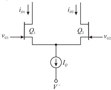
Figure 1
Calculation:
The expression for the current
The expression for the current
Both the JFET are matching so,
The expression to determine the value of the differential mode voltage is given by,
So the difference of current is,
The value of the sum of the drain current is given by,
So,
Square both the sides of the above equation.
Again square both the sides of the equation.
Solve further as,
The expression for the current
Conclusion:
Therefore, the expression for current ratios are
(b)
To show: The base current is switched to other transistor when
(b)
Explanation of Solution
Given:
The given circuit is shown in Figure 1
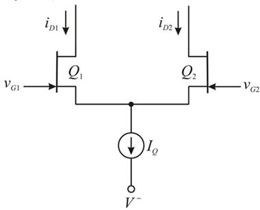
Figure 1
Calculation:
The diagram for the normalized dc transfer characteristics of MOSFET differential amplifier as a function of differential input voltage is shown in Figure 2
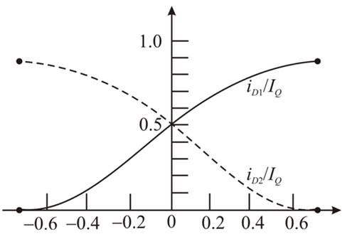
Figure 2
The expression to derive the expression for the differential input voltage is given by,
Therefore, the expression for the normalized differential voltage is given by,
Conclusion:
Therefore, the required expression is
(c)
To show: The expression for the maximum forward transconductance is
(c)
Explanation of Solution
Calculation:
The expression for the current
Differentiate both the sides of the equation.
Conclusion:
Therefore, the expression for conductance is
Want to see more full solutions like this?
Chapter 11 Solutions
Microelectronics: Circuit Analysis and Design


- Qla: which qudrant work The step down always working in first qudrant mod The step down properd to work in 3rd qudrant Q1/b: cyclo_convedter Cyclo converter minimaiz the harmonics rat due sequence wings actation Cyclo converter rectifiring the input AC voltage Q/c: Step up choppers One desadvantage of Step up is non zero starting O One advantage of Step up voltage is non zero starting O Q1ld: The triggering angle Theta determine the amount of Ton/Toff switching operation and duty cycle of source voltage out put power Q1/e:IGBT device biult in a combination of BJT & MOSFT UJT & Thyristorarrow_forwardQ- A buck converter feeding a variable resistive load is shown in the figure. The switching frequency of the switch S is 100 kHz and the duty ratio is 0.6. The output voltage Ve is 36 V, Assume that all the components are ideal, and that the output voltage is ripple-free. The value of R (in Ohm) that will make the inductor current (i) just continuous is 60 V + S 5 mH +1 Vo 36 Varrow_forwardQ1. Find the input impedance Zm(S) of each of the circuit in Figure Q1. ww 1H 1H 0.5 F 1F (a) (b) Figure Q1 all ll Harrow_forward
- A three phase full controlled converter is supplied by a phase voltage Vs-120V, 60 Hz. Consider a resistive load R=10 Q. If the RMS value of the output current is equal to 10.94A, then the RMS value of the input line current would be equal to: Select one: O a. 4.93A Ob. 2.93A OC. 6.93A O d. 8.93A TOSHIBAarrow_forwardQ2:-Find the output voltage Vo . Ry B2HF 100 kQ + 100 mV rms,arrow_forwardA step down converter is operated with a duty cycle of k = 0.75. The input voltage is Vs = 20V, and the load is: L = 5mH, R = 1502. The minimum inductor current is I₁ = 0.1A. The maximum inductor current is: Select one: a. 1.9 A b. None of these OC. 0.9 A O d. 1.1 A Oe. 2 Aarrow_forward
- For the circuit below and V1 waveform shown, plot Vout: U1 Vout OUT R1 OPAMP 1M V1 C5 20u Input voltage to circuit 15 12 6. 10 15 20 25 Time (msec) V1 (volts) 5/arrow_forwardSketch the DC load line for the fixed bias circuit and place the Q-point on it. - (1.24 MA, Io.76V) %3D Q - Peint Vcc =+12V RC 1k2 RB 1 MQ BC107 Vc VB Quantity Measured VB 0-6 28 volt 07-82 V1t 0.628 volt VC V BEQ IBQ 0-0000|13,A A 0-00418 A 0.782 Uolt IcQ V CEQ Bacarrow_forwardA boost converter has an input voltage Vb=5V. The average load current is lo=0.5A. The switching frequency is 25 kHz. Suppose that a regulator is added (L=0.15 mH and C=0.22 mF) and that the current is continuous. If the average output voltage is Vo =15V, then the duty cycle k is equal to: Select one: O a. 0.3 O b.0.67 c. None of these d. 0.5arrow_forward
- 4- Design a boost converter that will have an output of 60 V from a 24-V source. Design for continuous inductor current and an output ripple voltage of less than one percent. The load is a resistance of 50 2. Assume ideal components for this design. VL ooooo ip - ^arrow_forward1- In a buck DC/DC converter: ton Va = 100 V, R = 80, D ==0.8, f == 20000 Hz, L = 200 μH, Find: a) average voltage and current of the load Vala. b) maximum and minimum current of inductor. c) Voltage ripple of the capacitor. d) the average input current. e) draw the figure of the inductor current. C1 = 40 Micro farad Q Vd - İd K C1 ww + Voarrow_forwardIn an ideal, steady-state and uninterrupted current mode, a Buck-Type DC-DC converter has a load resistance of 20 ohms, an output power of 120W, and a relative ripple in coil current b. What is the coil value in this circuit? (D-0.35,f-10 kHz) a) L-63.7 mH b) L-64 microH c) L=33.7 mH d) L=64H e) L-66mHarrow_forward
 Introductory Circuit Analysis (13th Edition)Electrical EngineeringISBN:9780133923605Author:Robert L. BoylestadPublisher:PEARSON
 Delmar's Standard Textbook Of ElectricityElectrical EngineeringISBN:9781337900348Author:Stephen L. HermanPublisher:Cengage Learning
 Programmable Logic ControllersElectrical EngineeringISBN:9780073373843Author:Frank D. PetruzellaPublisher:McGraw-Hill Education
 Fundamentals of Electric CircuitsElectrical EngineeringISBN:9780078028229Author:Charles K Alexander, Matthew SadikuPublisher:McGraw-Hill Education
 Electric Circuits. (11th Edition)Electrical EngineeringISBN:9780134746968Author:James W. Nilsson, Susan RiedelPublisher:PEARSON
 Engineering ElectromagneticsElectrical EngineeringISBN:9780078028151Author:Hayt, William H. (william Hart), Jr, BUCK, John A.Publisher:Mcgraw-hill Education,