
Videos
a.
The value of
a.
Answer to Problem 11.46P
Explanation of Solution
Given:
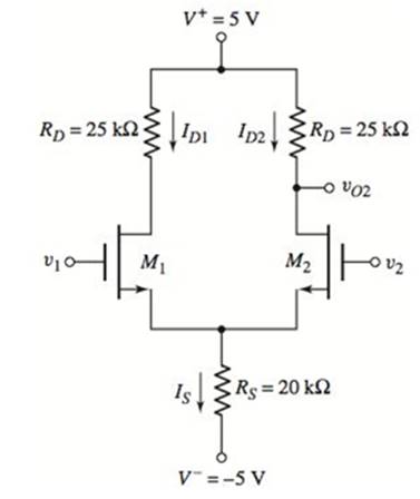
The given circuit is,
Calculation:
Consider the given figure,
Let calculate gate-to source voltage,
Now calculate source current,
Now find output voltage,
Hence,
b.
The differential-mode voltage gain and common-mode voltage gain along with CMRRdB
b.
Answer to Problem 11.46P
Explanation of Solution
Given:
The given circuit is,
Calculation:
Consider the small − signal equivalent circuit.
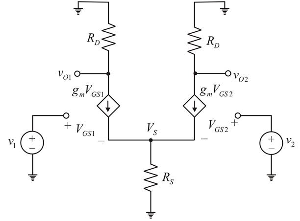
Apply KCL at node
Now,
Hence,
Want to see more full solutions like this?
Chapter 11 Solutions
Microelectronics: Circuit Analysis and Design


- N-channel Mosfet compared to P channel mosfetWhich of the following is true?A) It is faster.B) It has a lower input impedance.C) It has a lower noise level.D) nonearrow_forwardCalculate the output impedance for small-signal equivalent circuit. (R1=10 k ohm, r0, =10 k ohm)arrow_forwardExplain the following statements:(a) IG is zero amperes for a JFET transistor(b) High input resistance of a JFET(c) The application of a positive VGS of an n-channel D-MOSFET results in an ID exceeding IDSS.arrow_forward
- 26 Determine Vị and I, for the two-stage amplifier shown in the circult of Figure P11.26, with identical MOSFETS having K =1 A/V? and Vr =3V, for a. VG = 4 V, b. VG = 5 V c. VG = 4+0.1 cos(750) %3Darrow_forwardIn the BJT circuit below, assume VBE 0.6V and CE current gain ß very large. Then the collector voltage is? 33k 11k = 2k 1k 12Varrow_forwardQ1. The output characteristic of a typical transistor is shown below, where the quiescent point is selected on it. This transistor is used in the bias circuit presented below. Find the suitable values of Rg and Rc to fix the Q-point of the circuit properly. +Vcc = 12 V 12- Is = 70 uA 10- Ig = 60 uA 8- Rc Is = 50 uA Rs 6- Ig= 40 uA 4. Is = 30 uĄ Is = 20 uA B = 100 2- VBE = 0.7 V 0- -2- 2 4 6 8 10 12 14 16 VCE (V) Ic (mA)arrow_forward
- The transistor in Figure has parameters VTN= 0.4 V, k'n= 100 µA/N?, and W/L = 100. What are the values of R1 and R2 to have ID= 1 mA and Rin = 200 k2? VDD = 1.8 V RpD C 0.5 k2 R1 Rin R2arrow_forward4. For the transistor in the figure shown below, the parameters are ß = 100 and VÀ = ∞. a. Design the circuit such that lEQ = 1mA and the Q-pt is in the center of the dc load line. b. If the peak-to-peak sinusoidal output voltage is 4V, determine the peak-to-peak sinusoidal signals at the base of the transistor and the peak-to-peak value of Vs. If the load resistor R₁ = 1kQ is connected to the output through a coupling capacitor, determine the peak-to-peak value in the output voltage, assuming vs is equal to the value determined in part (b). Vcc=+10 V www Rs = 0.7 kΩ Cc www RB RE voarrow_forwardVcc-+15V RC1 RC2 5 k2 5 ka Vout Vo2 RB1 1 ka RB2 1 ka Q2 Vs2 Vs1 RE 7.5 ka VEE-15V Assume Ql and Q2 are identical transistors with B=hfec=100 and VBE-0.7V. Determine hiej and hiez. Determine the differential gains Ad, (for single-ended) and Ada (for double ended). Determine the common-mode gains Ac, (for single-ended) and Aca (for double ended). Determine the common-mode rejection ratio CMRR for single-ended output. Determine the common-mode rejection ratio CMRR for double-ended output.arrow_forward
- Consider two LTI systems (cascade) with the unit sample responses p1(x) and P2[x].Compute output g(x) ... please check the result as i done in Figurearrow_forwardElectrical Engineering Please solve ASAP 1. The figure shows a CE power amplifier in which the collector resistor serves also as the load resistor. Assume Boc = Be = 120. +12 V a) Determine the de Q-point (Icq and Vcr). Re 470 1 b) Determine the voltage gain and the power gain. R 12 kn c) The Quiescent power. 10 uF d) The i'p signal power 10 F RE 220 e) The output signal power. 400 mV pp 1.0 kHz ) The efficiency of the power amplifier. R2 4.7 k Ru 120 2 10 uF 470 1 Ba- Boc= 120arrow_forwardRe £ Value ZRB 꿀 Consider the transis BE=0.70 The Circuit has the Cirsuit Shown. Let B = 150 Cirbuit shown. and assume that shown .RB below PIRE Rc 47 ки base Current, IB Collector Current, I Mortage 74702 Is V 1201002 the Determine 3. Determine the Determine the Cmitter Vee Determine the value of RB that sets Vce = 0.3 V 2.3 between the Collector andarrow_forward
 Introductory Circuit Analysis (13th Edition)Electrical EngineeringISBN:9780133923605Author:Robert L. BoylestadPublisher:PEARSON
 Delmar's Standard Textbook Of ElectricityElectrical EngineeringISBN:9781337900348Author:Stephen L. HermanPublisher:Cengage Learning
 Programmable Logic ControllersElectrical EngineeringISBN:9780073373843Author:Frank D. PetruzellaPublisher:McGraw-Hill Education
 Fundamentals of Electric CircuitsElectrical EngineeringISBN:9780078028229Author:Charles K Alexander, Matthew SadikuPublisher:McGraw-Hill Education
 Electric Circuits. (11th Edition)Electrical EngineeringISBN:9780134746968Author:James W. Nilsson, Susan RiedelPublisher:PEARSON
 Engineering ElectromagneticsElectrical EngineeringISBN:9780078028151Author:Hayt, William H. (william Hart), Jr, BUCK, John A.Publisher:Mcgraw-hill Education,